Production Method for Semiconductor Device and Substrate Processing Apparatus

Active Publication Date: 2008-05-29
KOKUSA ELECTRIC CO LTD
View PDF3 Cites 254 Cited by
  • Summary
  • Abstract
  • Description
  • Claims
  • Application Information

AI Technical Summary

Benefits of technology

[0079]the plasma processing supplying an oxygen atom-containing gas into the processi

Problems solved by technology

However, in the thin film formed at a lower temperature (600° C. or lower), problems such as increase in etching speed (when film quality is checked, the produced film

Method used


Image

  • Production Method for Semiconductor Device and Substrate Processing Apparatus
  • Production Method for Semiconductor Device and Substrate Processing Apparatus
  • Production Method for Semiconductor Device and Substrate Processing Apparatus

Examples


Embodiment Construction

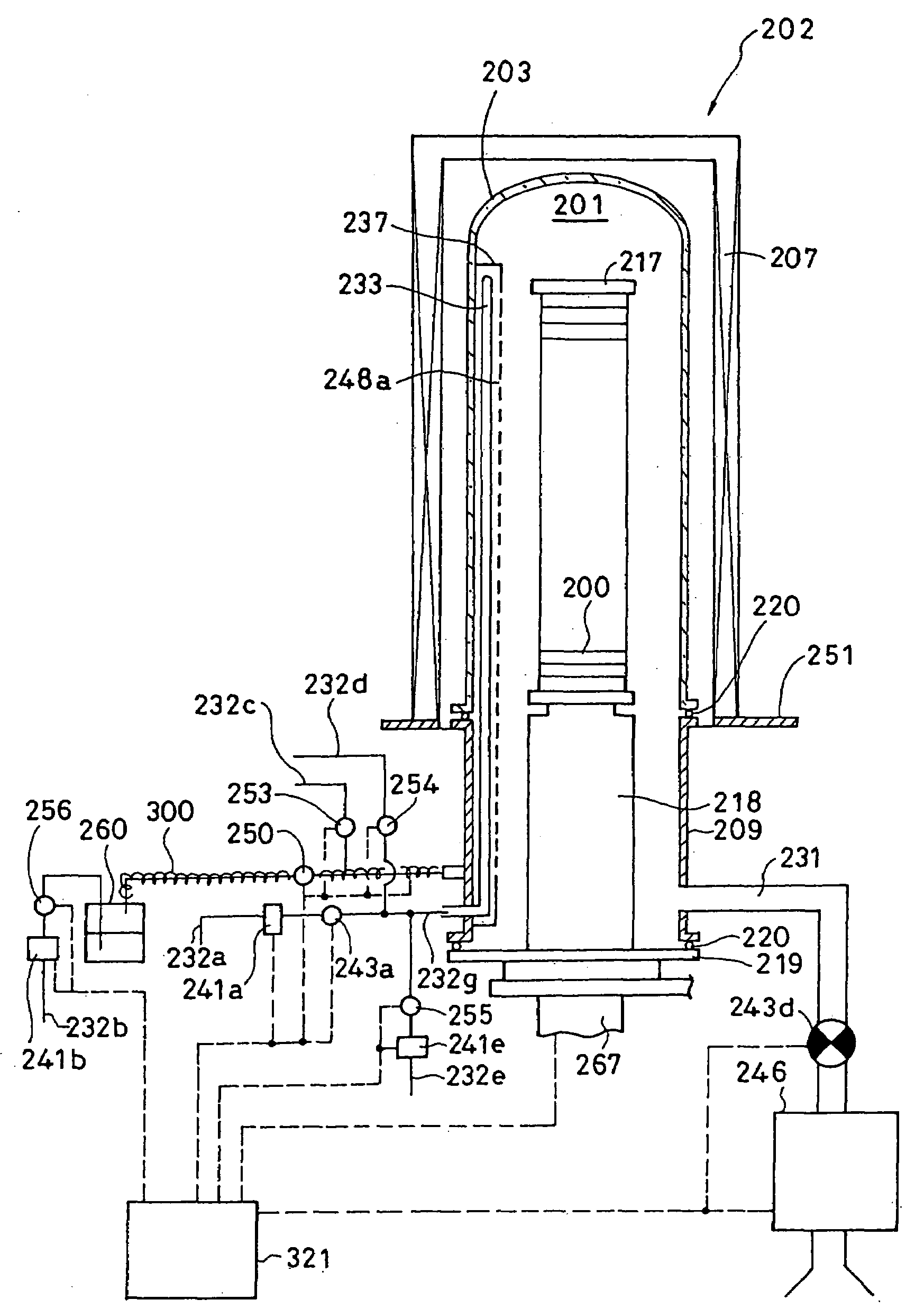
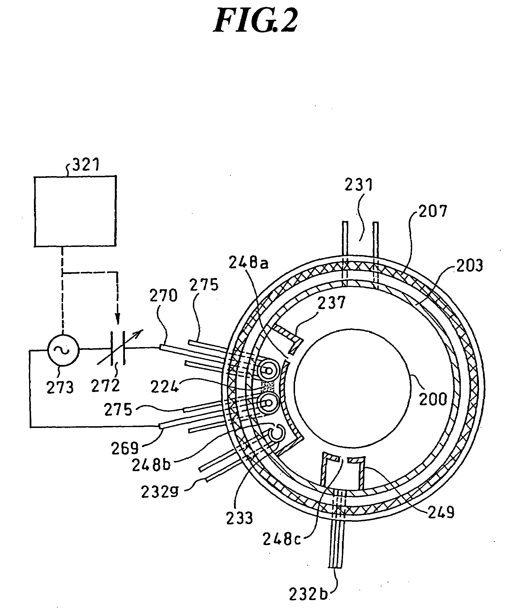
[0111]Next, preferred embodiments of the present invention will be explained.

[0112]In the preferred embodiments of the present invention, a film forming operation and plasma processing are continuously carried out in the same processing chamber to form a high quality film at a low temperature.

[0113]By doing like this, an ALD process can also be used easily. In the ALD method, a step of supplying a first reactant into a processing chamber accommodating a substrate therein and for allowing the first reactant to be absorbed on a surface of the substrate, a step of removing a surplus of the first reactant from the processing chamber, a step of supplying a second reactant into the processing chamber and for allowing the second reactant to react with the first reactant adsorbed on the surface of the substrate to form a thin film of at least one atomic layer, and a step of removing a surplus of the second reactant from the processing chamber are repeated a plurality of times, thereby depos...


PUM

PropertyMeasurementUnit
Pressureaaaaaaaaaa
Fractionaaaaaaaaaa
Fractionaaaaaaaaaa

Abstract

Disclosed is a producing method of a semiconductor device comprising a first step of supplying a first reactant to a substrate to cause a ligand-exchange reaction between a ligand of the first reactant and a ligand as a reactive site existing on a surface of the substrate, a second step of removing a surplus of the first reactant, a third step of supplying a second reactant to the substrate to cause a ligand-exchange reaction to change the ligand after the exchange in the first step into a reactive site, a fourth step of removing a surplus of the second reactant, and a fifth step of supplying a plasma-excited third reactant to the substrate to cause a ligand-exchange reaction to exchange a ligand which has not been exchange-reacted into the reactive site in the third step into the reactive site, wherein the first to fifth steps are repeated predetermined times.

Description

BACKGROUND OF THE INVENTION[0001]1. Field of the Invention[0002]The present invention relates to a producing method of a semiconductor device and a substrate processing apparatus.[0003]2. Description of the Related Art[0004]To produce a semiconductor device, a thin film such as a dielectric film, a metal oxide film or the like is formed on a semiconductor substrate at a low temperature by a CVD (Chemical Vapor Deposition) method or an ALD (Atomic Layer Deposition) method.[0005]However, in the thin film formed at a lower temperature (600° C. or lower), problems such as increase in etching speed (when film quality is checked, the produced film is etched and evaluated, and if the film is not dense, the etching speed is increased), and film shrinkage when high temperature process is carried out are generated. Therefore, a method and an apparatus for producing a high quality film are desired.SUMMARY OF THE INVENTION[0006]Hence, it is a main object of the present invention to provide a pr...

Claims


Application Information

Patent Timeline
IPC IPC(8): H01L21/469C23C16/52
CPCC23C16/345H01L21/3185C23C16/45536C23C16/45546C23C16/509H01L21/0214H01L21/0217H01L21/02178H01L21/02211H01L21/02274H01L21/0228H01L21/02332H01L21/0234H01L21/3141H01L21/3162C23C16/403H01L21/205H01L21/203H01L21/31
Inventor MIYA, HIRONOBUTOYODA, KAZUYUKIMIZUNO, NORIKAZUSATO, TAKETOSHISAKAI, MASANORIASAI, MASAYUKIOKUDA, KAZUYUKIHORITA, HIDEKI
Owner KOKUSA ELECTRIC CO LTD
Why Eureka
Try Eureka