

Photoconductor for electrophotography
a photoconductor and electrophotography technology, applied in the field of photoconductor, can solve the problems of deteriorating image quality, less light available to expose the surface of the photoconductor, and conventional photoconductors to have poor photoresponse, so as to reduce the preservability of electrically charged surface potential, increase sensitivity, and increase the effect of sensitivity
Inactive Publication Date: 2000-04-04
FUJI ELECTRIC CO LTD
View PDF5 Cites 3 Cited by
- Summary
- Abstract
- Description
- Claims
- Application Information
AI Technical Summary
Benefits of technology
It is a further object of the invention to provide a photoconductor having improved resolution and sensitivity.
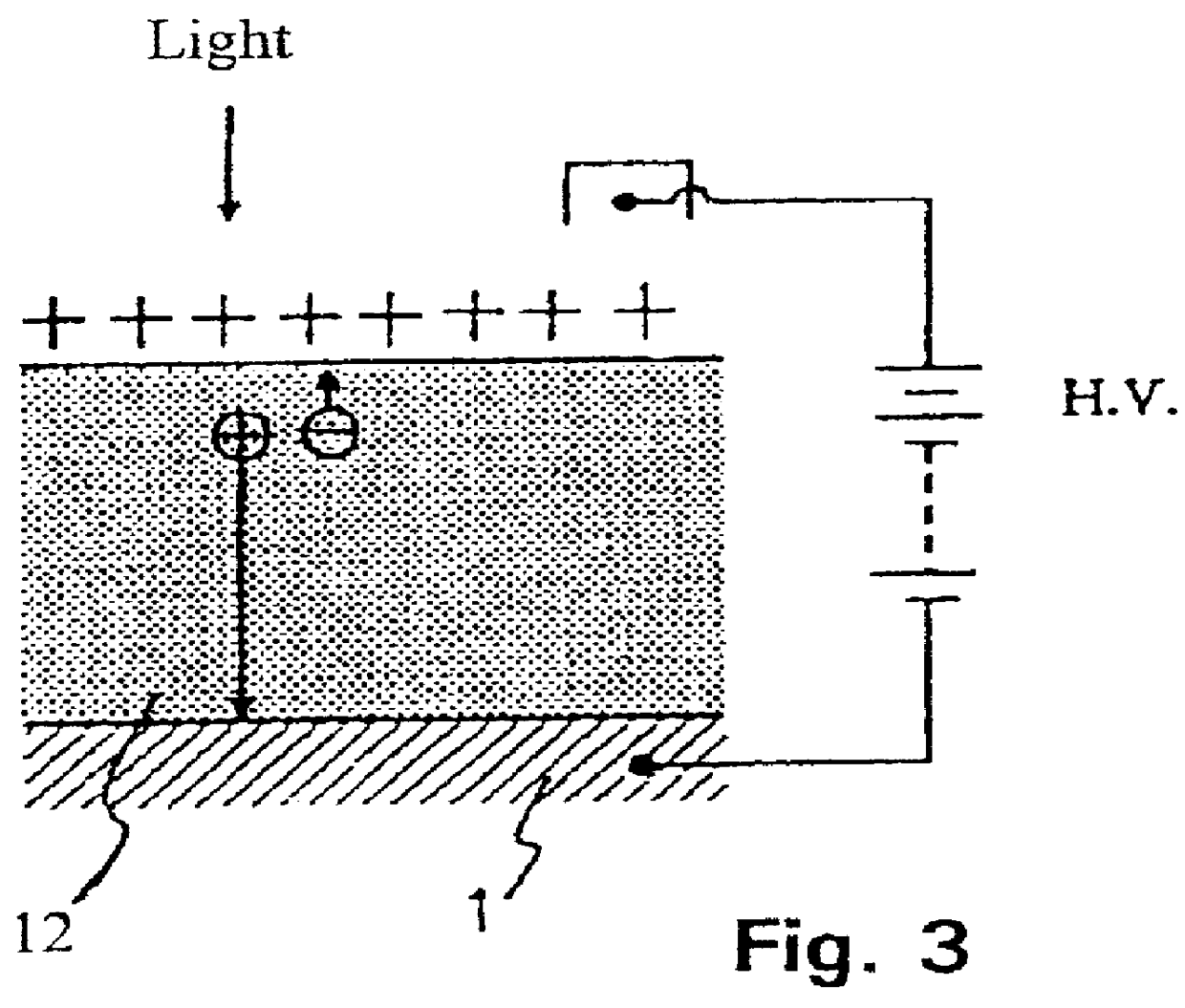
The multilayered photosensitive coating is heat treated after vacuum deposition. Heat treatment facilitates an even distribution of iodine in the photosensitive layers. Heat treatment of the photosensitive layers preferably is performed in a preferred range of between 100.degree. to 200.degree. for 30 to 80 minutes. The surface roughness (Rmax.) of the conductive substrate is 0.5 .mu.m or less. Larger surface roughnesses (Rmax.) leads to point defects in the images. These defects will be present even if a low surface potential is applied to the photoconductor as mentioned above. Because of their good workability, aluminum alloys are preferred for the conductive substrate.
Problems solved by technology
The problem with electrostatic latent image formation is that the higher the print speed, namely the larger the rotational velocity of the photoconductor, the less light is available to expose the surface of the photoconductor.
The short time available for decay leads to deteriorating image quality along with patent image disorders such as image contrast problems etc.
Low mobility of carriers and long potential decay periods cause conventional photoconductors to have poor photoresponses.
This results in deterioration of image quality when applied to high speed devices.
However, because conventional photosensitive coatings are so thick, incident light causes the generated carriers to move transversely.
This causes the images to blur and fade.
On the other hand, reducing the thickness of the photosensitive coating poses practical problems.
Thin photosensitive coatings cause white or black point defects to appear on the images.
These defects are caused by burrs left on the substrate during the cutting process.
Additionally, conventional photoconductors lack the sensitivity required for high speed devices.
Method used
View moreImage
Smart ImageViewing Examples

Examples
example 2
The photoconductor in Example 2 is prepared in the same manner as Example 1 except that the first layer is 50 .mu.m thick. This produces a multilayered photosensitive coating that is 60 .mu.m thick.
Login to View More PUM
| Property | Measurement | Unit |
|---|---|---|
| thick | aaaaa | aaaaa |
| thick | aaaaa | aaaaa |
| thickness | aaaaa | aaaaa |
Abstract
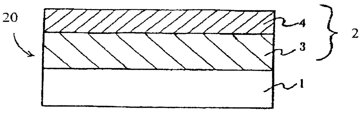
A first selenium-arsenic layer of a photoconductor, deposited on a conductive substrate, has a thickness and arsenic concentration effective to preserve an electrically charged surface potential in darkness and to transport carriers generated on exposure to light. The first layer is between 20 to 70 mu m thick. A second amorphous selenium-arsenic alloy layer, formed on the first layer, generates carriers on exposure to light. The surface roughness, Rmax., of the conductive substrate is less than or equal to 0.5 mu m. The first layer, or both of the photoconductive layers, are doped with iodine. When both layers contain iodine, the iodine content of the second layer is equal to or less than that of the first layer. The thickness of the second layer is between 5 to 30 mu m. The arsenic content of the amorphous selenium-arsenic alloy of the second layer is equal to or greater than that in the first layer. After deposition of the first and second layers, the photoconductor is heat treated at between 100 DEG to 200 DEG for 30 to 80 minutes. In a further embodiment the first layer of the photoconductor has an arsenic content in the range of 10 to 45 wt %. The second layer arsenic content is in the range of 25 to 45 wt %.
Description
The present invention relates to a photoconductor for electrophotography, which is central to electrophotographic devices, including copiers, printers, and facsimiles etc. In particular, the present invention relates to photoconductors utilized in high speed (100 A4 size sheets per minute or faster), high resolution (dot densities of 300 dpi or more) electrophotographic applications.In recent years, the focus of research and development in electrophotographic devices such as copiers, printers, and facsimiles, etc. has been on developing higher print speeds and higher resolutions. Conventional electrophotographic devices have a print speed ranging from 40 to 100 sheets per minute on A4 size paper. Additionally, electrophotographic devices that employ photoconductors made of amorphous selenium, particularly amorphous selenium-arsenic alloys, have dot densities of 240 dpi or less. Photoconductors made of amorphous selenium exhibit excellent resistance to printing fatigue.Photoconductor...
Claims
Login to View More Application Information
Patent Timeline
 Patent Type & AuthorityPatents(United States)
IPC IPC(8): G03G5/043G03G5/082G03G5/08G03G5/00G03G5/10
CPCG03G5/08207G03G5/0433
InventorARAI, AKIOKINA, HIDEKI
OwnerFUJI ELECTRIC CO LTD