Linear voltage regulator
- Summary
- Abstract
- Description
- Claims
- Application Information
AI Technical Summary
Benefits of technology
Problems solved by technology
Method used
Image

Examples
Embodiment Construction
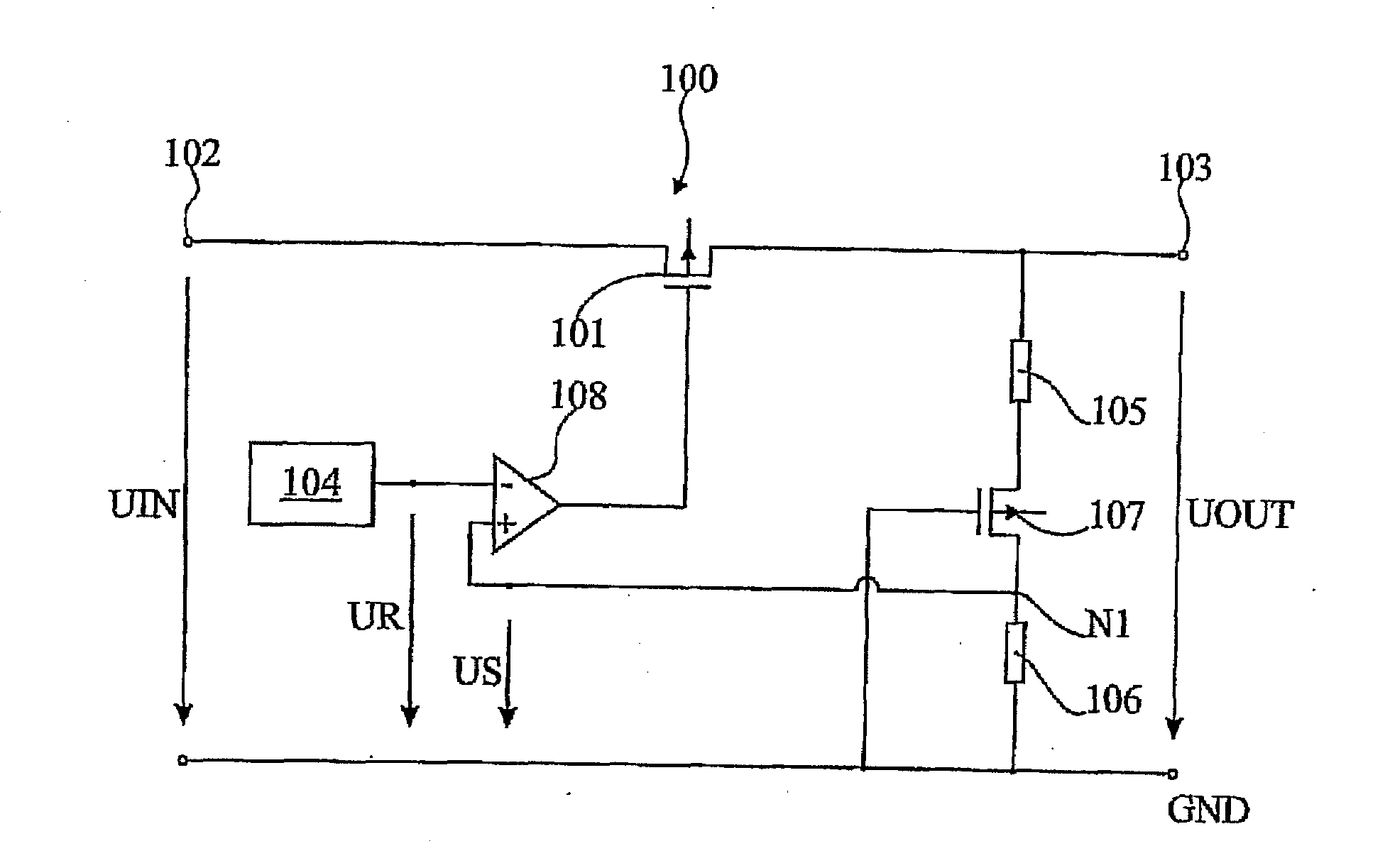
[0028]FIG. 1 shows a schematic diagram of a linear voltage regulator 100 according to the invention. The linear voltage regulator 100 includes a first normally-off PMOS transistor 101, with this transistor or its drain-source path being connected between a terminal 102 for an input voltage UIN and a terminal 103 for an output voltage UOUT, a reference voltage source in the form of a band-gap reference 104 for producing a reference voltage UR, a first resistor 105, a second resistor 106, a second normally-off PMOS transistor 107, and a differential amplifier 108 having an inverting input and a non-inverting input.
[0029]The first resistor 105, the second transistor 107 or its drain-source path, and the second resistor 106 are connected in series in this sequence between the terminal 103 for an output voltage UOUT and a reference voltage in the form of the ground potential GND. The first resistor 105, the second transistor 107, and the second resistor 106 form a voltage divider, with a...
PUM
 Abstract
Description
Claims
Application Information