
Method for Making a Keyhole Opening during the Manufacture of a Memory Cell

a memory cell and keyhole technology, applied in the manufacturing of semiconductor/solid-state devices, basic electric elements, electric devices, etc., can solve the problems of high density memory devices, lack of uniformity or reliability, limited cell manufacturing processes of standard integrated circuit manufacturing processes, etc., to reduce the size not increase the volume of the second layer, and increase the volume of the first opening segmen

Active Publication Date: 2008-06-12
MACRONIX INT CO LTD
View PDF70 Cites 64 Cited by
  • Summary
  • Abstract
  • Description
  • Claims
  • Application Information

AI Technical Summary

Benefits of technology

[0014]Another example of a method for creating a keyhole opening during the manufacture of a memory cell comprises forming a base layer having a bottom electrode. Materials for first and second layers that increase and decrease their respective volumes when subjected to a chosen process are selected. An upper layer is formed on the base layer with the second layer formed over the base layer and the first layer formed over the second layer. An opening is formed through the upper layer to expose a surface of the bottom electrode and to create a first memory cell subassembly. The opening comprises a first, upper opening segment formed within the first layer and a second opening segment formed within the second layer, the first and second opening seg

Problems solved by technology

One problem associated with phase change memory devices arises because the magnitude of the current required for reset operations depends on the volume of phase change material that must change phase.
Thus, cells made using standard integrated circuit manufacturing processes have been limited by the minimum feature size of manufacturing equipment.
Thus, techniques to provide sublithographic dimensions for the memory cells must be developed, which can lack uniformity or reliability needed for large scale, high density memory devices.

Method used


Image

  • Method for Making a Keyhole Opening during the Manufacture of a Memory Cell
  • Method for Making a Keyhole Opening during the Manufacture of a Memory Cell
  • Method for Making a Keyhole Opening during the Manufacture of a Memory Cell

Examples


Embodiment Construction

[0024]The following description of the invention will typically be with reference to specific structural embodiments and methods. It is to be understood that there is no intention to limit the invention to the specifically disclosed embodiments and methods but that the invention may be practiced using other features, elements, methods and embodiments. Preferred embodiments are described to illustrate the present invention, not to limit its scope, which is defined by the claims. Those of ordinary skill in the art will recognize a variety of equivalent variations on the description that follows. Like elements in various embodiments are commonly referred to with like reference numerals.

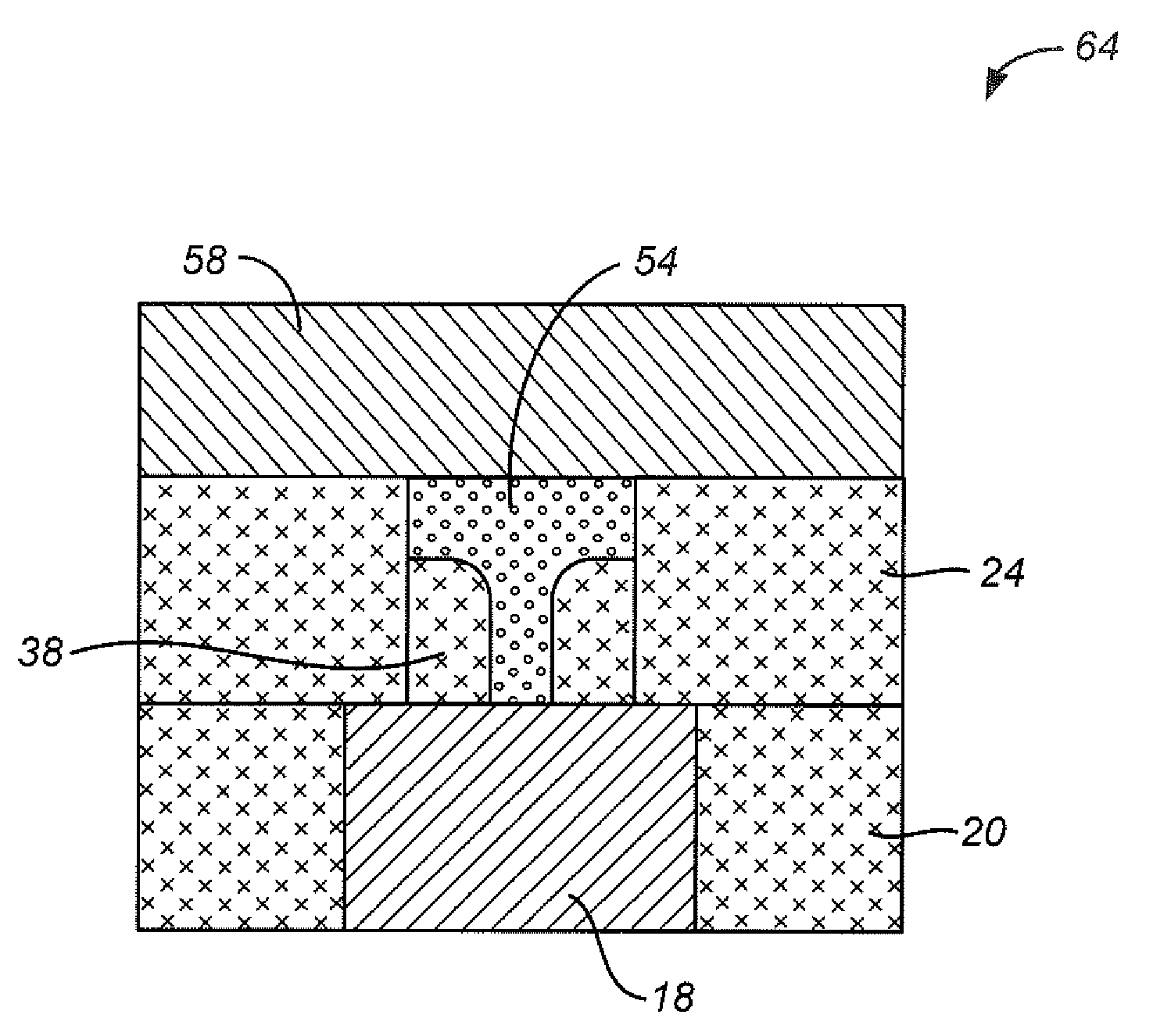
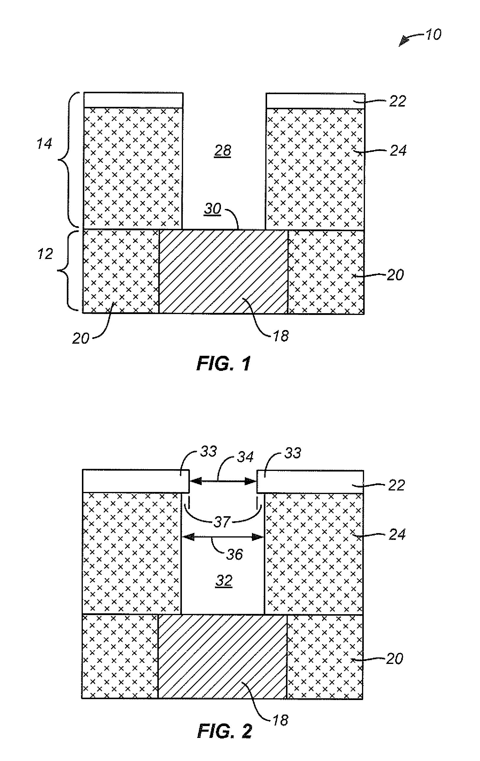
[0025]FIG. 1 is a simplified side view of a first memory cell subassembly 10 including a base layer 12 and an upper layer 14. Base layer 12 includes a bottom electrode 18 within an oxide layer 20. Bottom electrode 18 is typically made of TiN or tungsten while oxide layer 20 is typically made of silicon d...


PUM


Abstract

A keyhole opening is formed during one example of manufacturing a memory cell. An upper layer is formed on a base layer, the base layer having a bottom electrode. The upper layer includes a second layer formed over the base layer and a first layer formed over the second layer. A keyhole opening is formed through the upper layer to expose a surface of the bottom electrode and to create a first memory cell subassembly. The keyhole opening comprises a first, upper opening segment formed within the first layer and a second opening segment formed within the second layer, the first and second opening segments having first and second widths. The first layer has an overhanging portion extending into the opening so that the first width is shorter than the second width.

Description

CROSS-REFERENCE TO OTHER APPLICATIONS[0001]This application is related to the following US patent applications, each filed on the same day as this application, assigned to the same assignee and having the same inventor: Method for Making a Self-Converged Void and Bottom Electrode for Memory Cell, attorney docket number MXIC 1761-1 and Method for Making a Self-Converged Memory Material Element for Memory Cell, attorney docket number MXIC 1772-1PARTIES TO A JOINT RESEARCH AGREEMENT[0002]International Business Machines Corporation, a New York corporation; Macronix International Corporation, Ltd., a Taiwan corporation, and Infineon Technologies A.G., a German corporation, are parties to a Joint Research Agreement.BACKGROUND OF THE INVENTION[0003]1. Field of the Invention[0004]The present invention relates to high density memory devices based on memory materials, for example resistor random access memory (RRAM) devices, and to methods for manufacturing such devices. The memory material i...

Claims


Application Information

Patent Timeline
IPC IPC(8): H01L45/00
CPCH01L45/04H01L45/06H01L45/1233H01L45/1246H01L45/1683H01L45/144H01L45/146H01L45/147H01L45/1625H01L45/14H10N70/828H10N70/20H10N70/881H10N70/8836H10N70/231H10N70/026H10N70/066H10N70/8828H10N70/8833H10N70/826
Inventor LUNG, HSIANG LAN
Owner MACRONIX INT CO LTD
Features
  • Generate Ideas
  • Intellectual Property
  • Life Sciences
  • Materials
  • Tech Scout
  • Unparalleled Data Quality
  • Higher Quality Content
  • 60% Fewer Hallucinations
Learn More