Semiconductor integrated circuit

a technology of integrated circuits and semiconductors, applied in the direction of semiconductor devices, electrical equipment, transistors, etc., can solve the problems of difficult to improve the simulation accuracy of circuit simulators, large characteristic differences, and so as to minimize characteristic fluctuation, reduce simulation errors, and prevent characteristic fluctuation of transistors

Active Publication Date: 2008-06-19
CONVERSANT INTPROP MANAGEMENT INC
View PDF4 Cites 14 Cited by
  • Summary
  • Abstract
  • Description
  • Claims
  • Application Information

AI Technical Summary

Benefits of technology

[0016]As described above, among the transistors of the single well, by equalizing the distances from the well boundary to the centers of the active regions thereof, the influence of the well proximity effect can be prevented from varying among the transistors with different sizes, thereby minimizing characteristic fluctuation caused by the influence of the well proximity effect. Moreover, with the semiconductor integrated circuit according to the present invention, characteristic fluctuation of the transistor can be prevented which results from process variations, modeling error caused in the case where for the circuit simulator the influence of the well proximity effect is taken into consideration, and the like. This makes simulation error smaller on the LSI level or the block level, so that a decrease in the design period can be attained and in addition an increase in development cost can be prevented.
[0017]As is apparent from the above, with the semiconductor integrated circuit of the present invention, after determination of process conditions for each generation, the influence of the well proximity effect can be made equal on each of the transistors in the single well. Therefore, highly accurate circuit simulation can be performed even without carrying out the step of evaluating characteristic fluctuation and performing modeling. Also in the case where for the circuit simulator the influence of the well proximity effect is taken into consideration, the influence of relative characteristic fluctuation caused by simulation error due to modeling error, process variations, or the like can be suppressed.
[0018]Accordingly, highly accurate circuit simulation can be performed to prevent increases in development period and development cost.

Problems solved by technology

With rapid miniaturization of semiconductor integrated circuits, layout pattern, arrangement, and the like of circuit elements have been diversified and complicated in system LSIs (Large Scale Integrations) and the like.
Because of this trend, in development of such system LSIs, it becomes difficult to improve the simulation accuracy of a circuit simulator.
However, with recent miniaturization of elements, a problem has arisen that a large characteristic difference occurs between an ideal single transistor used to extract model parameters and a CMOS (Complementary Metal Oxide Semiconductor)-type transistor arranged in a cell widely used in actual design.
One of such problems includes characteristic fluctuation of a transistor resulting from the well proximity effect.
However, it is feared that such reflection of the modeled characteristic fluctuation to the circuit simulator increases simulation time and development time.
Furthermore, the range affected by the well proximity effect is as large as several micrometers, so that highly accurate modeling within realistic simulation time is difficult.
However, with this simulation, it is difficult to evaluate the transistor characteristics in a short time, which is likely to cause lengthening of development time and an increase in development cost.

Method used


Image

  • Semiconductor integrated circuit
  • Semiconductor integrated circuit
  • Semiconductor integrated circuit

Examples


first embodiment

[0027]Hereinafter, a semiconductor integrated circuit and its design method according to a first embodiment of the present invention will be described with reference to the accompanying drawings.

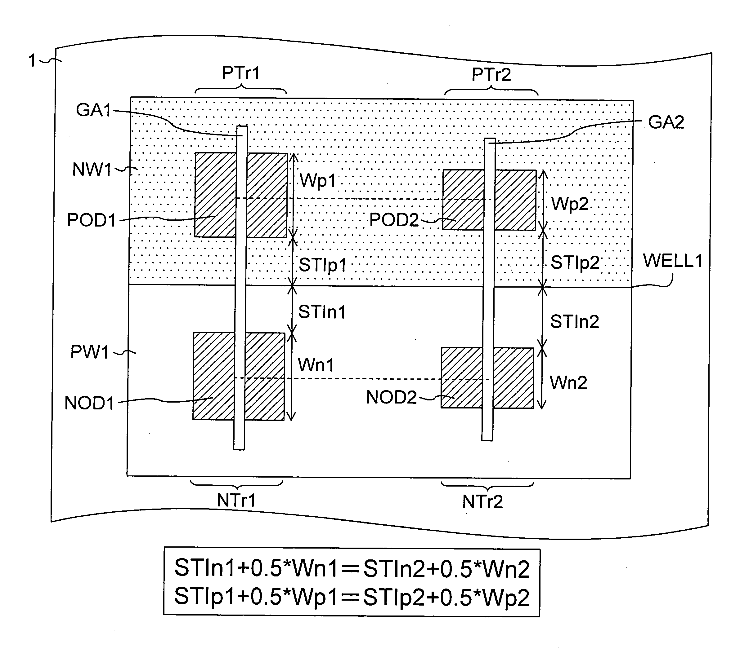
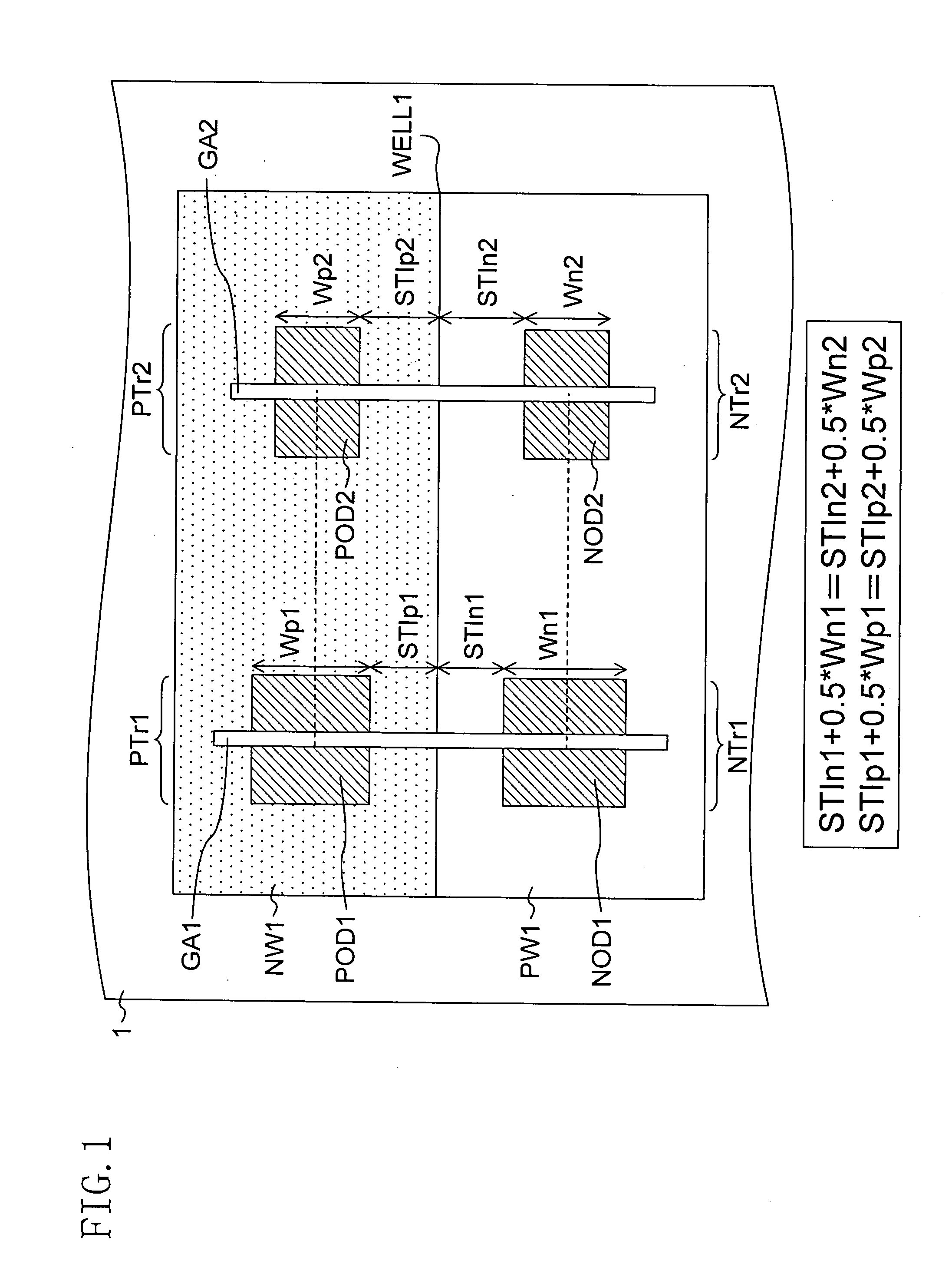
[0028]FIG. 1 is a plan view schematically showing a standard cell constituting the semiconductor integrated circuit according to the first embodiment of the present invention. In the specification and the scope of claims of the present invention, the standard cell indicates the area where CMIS transistors and the like are arranged and connected in order to implement one function or multiple functions (logic inversion, AND, and the like).

[0029]Referring to FIG. 1, in the semiconductor integrated circuit according to the first embodiment, an n-type well NW1 and a p-type well PW1 in contact with the n-type well NW1 at a well boundary WELL1 extending in the gate length direction are provided in a substrate 1 made of silicon or the like.

[0030]P-type active regions POD1 and POD2 having lengths in ...

second embodiment

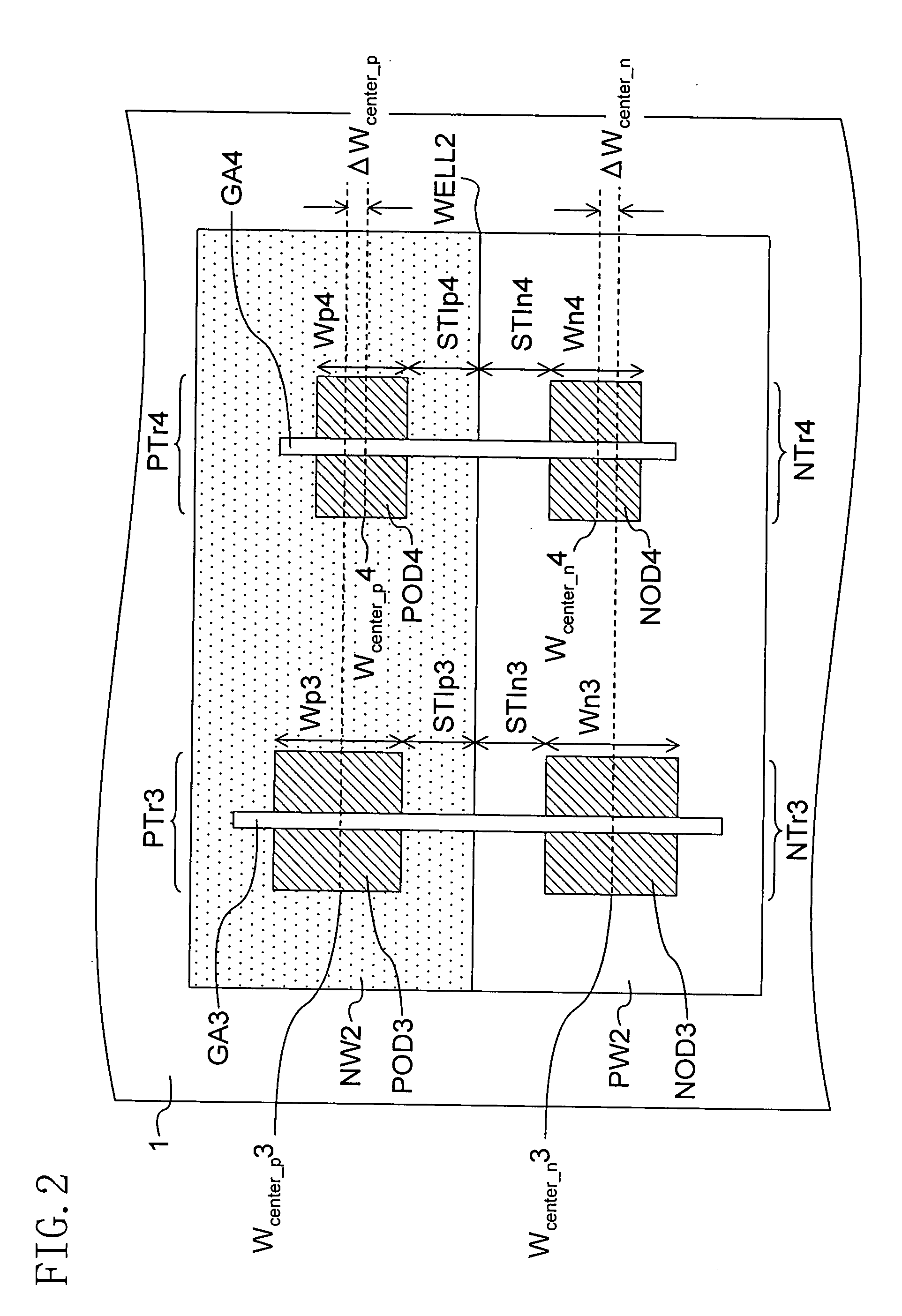
[0044]FIG. 4 is a plan view showing the structure of a standard cell constituting a semiconductor integrated circuit according to a second embodiment of the present invention. In the semiconductor integrated circuit according to the second embodiment, each of wells in the standard cell is provided with three transistors having different sizes, respectively.

[0045]Referring to FIG. 4, p-type active regions POD5, POD6, and POD7 having gate widths of Wp5, Wp6, and Wp7, respectively, are arranged in an n-type well NW3 formed in a substrate 1. Also, n-type active regions NOD5, NOD6, and NOD7 having gate widths of Wn5, Wn6, and Wn7, respectively, are arranged in a p-type well PW3 formed in the substrate 1. Above the p-type active regions POD5, POD6, and POD7 and the n-type active regions NOD5, NOD6, and NOD7, gate interconnects GA5, GA6, and GA7 are provided with respective gate insulating films (not shown) interposed therebetween.

[0046]P-channel transistors PTr5, PTr6, and PTr7 are provid...

third embodiment

[0053]FIG. 5 is a plan view showing the structure of a standard cell constituting a semiconductor integrated circuit according to a third embodiment of the present invention.

[0054]As shown in FIG. 5, in the standard cell according to the third embodiment, an n-type well NW4, a p-type well PW4 in contact at the well boundary WELL4 with the n-type well NW4, a p-type well PW5 in contact with the p-type well PW4, and an n-type well NW5 in contact at the well boundary WELL5 with the p-type well PW5 are sequentially formed in a substrate 1 from top to bottom in the gate width direction. Although the p-type well PW4 and the p-type well PW5 are separately provided in the third embodiment, a single p-type well may be provided instead of them.

[0055]P-type active regions POD8 and POD9 having gate widths of Wp8 and Wp9 (Wp8>Wp9) are arranged in the n-type well NW4, and n-type active regions NOD8 and NOD9 having gate widths of Wn8 and Wn9 (Wn8>Wn9) are arranged in the p-type well PW4. The n-type...


PUM


Abstract

An integrated circuit includes: a first well of a first conductivity type; a second well of a second conductivity type coming into contact with the first well at a well boundary extending in a gate length direction; a first transistor having a first active region of the second conductivity type provided in the first well; and a second transistor which has a second active region of the second conductivity type provided in the first well and differing from the first active region in length in a gate width direction. The center location of the first active region in the gate width direction is aligned with the center location of the second active region in the gate width direction with reference to the well boundary.

Description

BACKGROUND OF THE INVENTION[0001](a) Fields of the Invention[0002]The present invention relates to semiconductor integrated circuits made by integrating a great number of MIS transistors.[0003](b) Description of Related Art[0004]With rapid miniaturization of semiconductor integrated circuits, layout pattern, arrangement, and the like of circuit elements have been diversified and complicated in system LSIs (Large Scale Integrations) and the like. Because of this trend, in development of such system LSIs, it becomes difficult to improve the simulation accuracy of a circuit simulator.[0005]Typically, from a mask layout of a designed cell, information on connection between elements such as transistors, capacitors, and resistors, and in addition information on element characteristics such as transistor size, parasitic capacitance, parasitic resistance, and the like are extracted as a net list using a layout parameter extraction (abbreviated hereinafter as “LPE”) of a circuit, and the ext...

Claims


Application Information

Patent Timeline
Patent Type & Authority Applications(United States)
IPC IPC(8): H01L27/092
CPCH01L21/82385H01L27/0922H01L27/0207H01L21/823892
Inventor WATANABE, SHINJIIKOMA, DAISAKUYAMASHITA, KYOJIOOTANI, KATSUHIRO
Owner CONVERSANT INTPROP MANAGEMENT INC
Why Eureka
Try Eureka