Data processing apparatus and method for converting data values between endian formats

a data processing apparatus and data value technology, applied in the direction of electric digital data processing, program control, instruments, etc., can solve the problems of limiting the speed at which the data processing apparatus can be run, complex swizzle circuitry, etc., to reduce the complexity of swizzle circuitry on the critical path, improve the speed of operation, and reduce the complexity of swizzle circuitry. , the effect of improving the speed of operation

Active Publication Date: 2008-06-19
ARM LTD
View PDF2 Cites 21 Cited by
  • Summary
  • Abstract
  • Description
  • Claims
  • Application Information

AI Technical Summary

Benefits of technology

[0012]By such an approach, the swizzle circuitry is optimised to rapidly perform the required endian conversion for data values of the first predetermined size, at the expense of requiring additional time to perform the required endian conversion for data values which are not of that first predetermined size. This enables a reduction in the complexity of the circuitry provided on the critical path, because the swizzling is done speculatively expecting the data values to be of the first predetermined size. Hence the timing of the path when handling data values of the first predetermined size is significantly reduced, thereby improving the speed of operation when handling such data values.
[0013]In one embodiment, the second swizzle circuitry is arranged to perform the additional reordering operation in at least one clock cycle subsequent to a clock cycle in which the reordered data is produced by the first swizzle circuitry, whereby if the at least one data value is of said first predetermined size, the swizzle circuitry converts each data value in the block from the first endian format to the second endian format at least one clock cycle more quickly than if the at least one data value is of a size other than said first predetermined size. By allowing the additional re-ordering operation performed by the second swizzle circuitry to take place in at least one subsequent clock cycle, the clock speed is no longer constrained by the need to perform all possible swizzling re-ordering within the same clock cycle. In one embodiment, the first swizzle circuitry does not take an entire clock cycle to perform the re-ordering operation, and accordingly the operation of the first swizzle circuitry can be included within a clock cycle where other actions are taken, for example being included within the cycle in which the data is read from the first circuitry.
[0014]In one particular embodiment, the first swizzle circuitry is arranged to perform the reordering operation in a first clock cycle, and the second swizzle circuitry is arranged to perform the additional reordering operation in a next clock cycle, whereby if the at least one data value is of said first predetermined size, the swizzle circuitry converts each data value in the block from the first endian format to the second endian format one clock cycle more quickly than if the at least one data value is of a size other than said first predetermined size. Hence, the clock speed can be increased relative to a prior art system where the swizzle circuitry required sufficient multiplexing logic to allow all possible swizzle operations to be performed within a single cycle. Instead, the complexity of the swizzle circuitry on the critical path can be reduced, in that it now only needs to perform endian conversion assuming the data values to be of one fixed size, namely the first predetermined size, and if the data values are in fact of that first predetermined size, the endian conversion operation is completed as soon as the re-ordering operation performed by the first swizzle circuitry has been performed. The additional circuitry required to deal with data value sizes other than the first predetermined size is then placed off the critical path, and such additional re-ordering can be performed in the next clock cycle. For embodiments where the vast majority of the data values handled are of the first predetermined size, this can give rise to significant performance improvements. Further, in one embodiment, it has been found that for data values that are not of the first predetermined size, an additional clock cycle is already required for accessing those data values in any event, and accordingly there is no additional impact in requiring the second swizzle circuitry to perform the additional re-ordering operation in the next clock cycle.
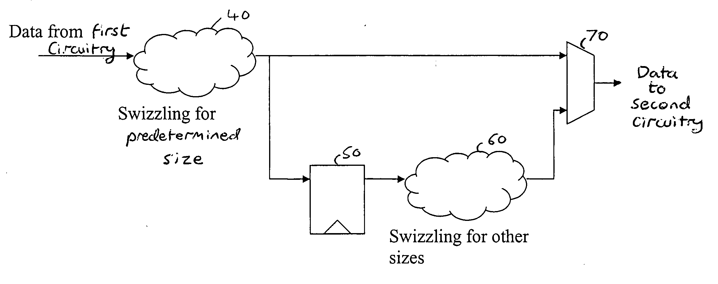
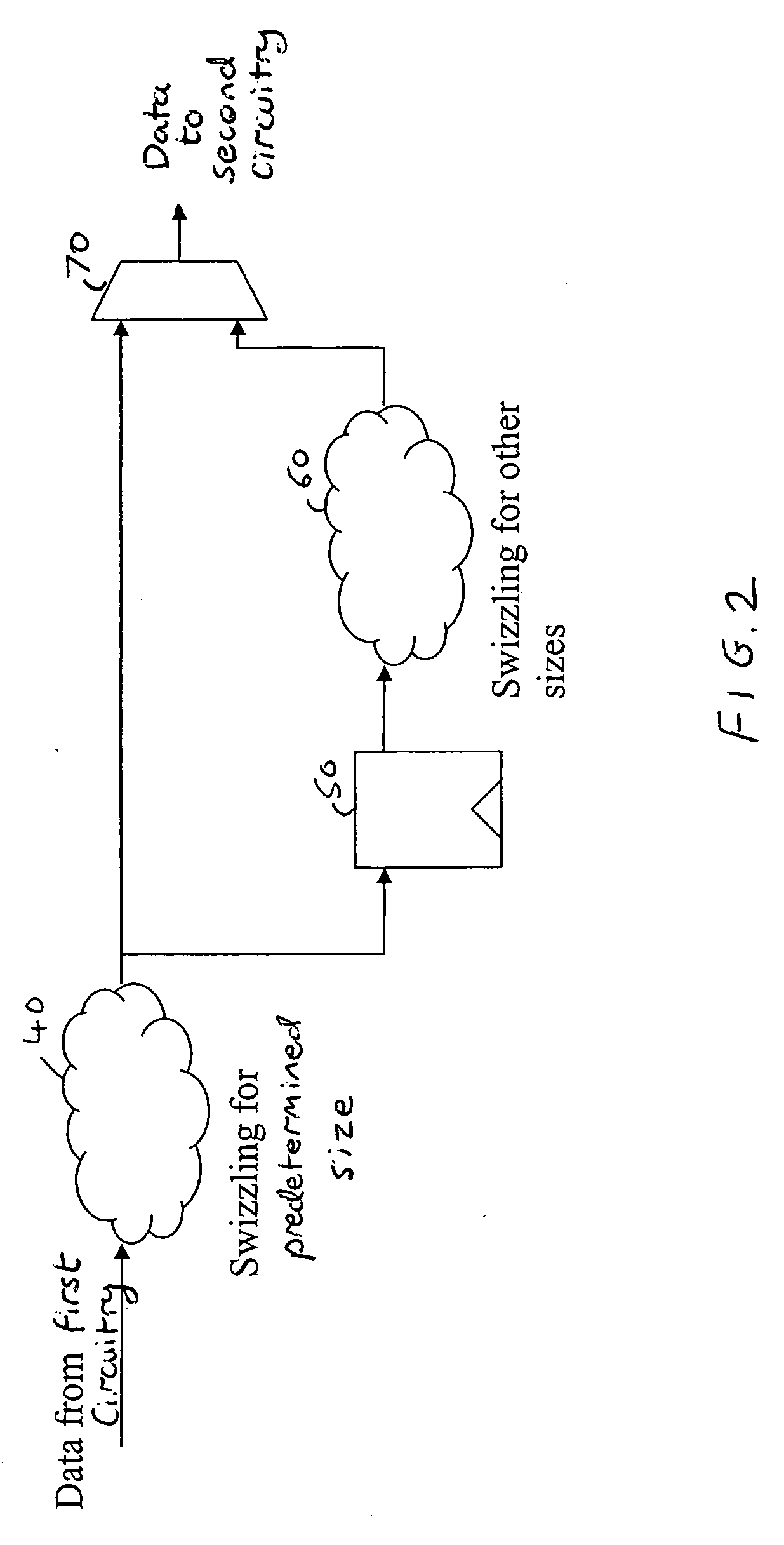
[0015]In one embodiment, the swizzle circuitry provides two data paths, a first data path passing from an input through the first swizzle circuitry to an output, and a second data path passing from the input through the first swizzle circuitry and the second swizzle circuitry to the output, data routed through the second path taking at least one cycle longer to reach the output than data routed through the first path. Hence, in such embodiments, the first data path provides a fast data path for performing endian conversion of data values of the first predetermined size.

Problems solved by technology

An added complexity is that the data values operated upon within a data processing apparatus can be of various different sizes, and the exact re-ordering required when performing endian conversion will be dependent on the size of the data values being handled at the time.
Due to the need to cater for data values of various different sizes, the swizzle circuitry becomes complex, and for example will include many multiplexers that add propagation delay to the data path.
For certain paths where such swizzle circuitry is required, the complexity of the swizzle circuitry can lead to those paths becoming a critical path within the data processing apparatus, thereby limiting the speed at which the data processing apparatus can be run.
Such a path may represent a critical timing path, with the complexity of the swizzle circuitry contributing to the delay in that path.

Method used


Image

  • Data processing apparatus and method for converting data values between endian formats
  • Data processing apparatus and method for converting data values between endian formats
  • Data processing apparatus and method for converting data values between endian formats

Examples


Embodiment Construction

[0034]FIG. 1 is a block diagram of a data processing apparatus in accordance with one embodiment of the present invention. As shown in FIG. 1, the data processing apparatus has first circuitry 10 which employs a first endian convention. Similarly, second circuitry 30 is provided which employs a second endian convention. Hence, if the first circuitry employs the little-endian convention, the second circuitry employs big-endian convention, and conversely if the first circuitry employs the big-endian convention, the second circuitry employs the little-endian convention. If data is to be passed from the first circuitry to the second circuitry 30, then an endian conversion operation will be required in order to enable the second circuitry to correctly interpret the data it receives from the first circuitry 10. This endian conversion operation is performed by the swizzle circuitry 20.

[0035]The swizzle circuitry 20 of FIG. 1 is illustrated in more detail in FIG. 2. As shown in FIG. 2, the ...


PUM


Abstract

A data processing apparatus and method are provided for converting data values from a first endian format to a second endian format. Swizzle circuitry is provided within the data processing apparatus for receiving a block of data containing at least one data value, and for converting each data value in the block from the first endian format to the second endian format. The swizzle circuitry comprises first swizzle circuitry for performing a re-ordering operation on the block of data assuming the at least one data value contained therein is of a first predetermined size, in order to produce re-ordered data. Further, second swizzle circuitry is provided which is responsive to an indication that the at least one data value is of a size different to the first predetermined size to perform an additional re-ordering operation on the re-ordered data having regard to the size of the at least one data value in order to convert each data value to the second endian format. The swizzle circuitry is responsive to an indication that the at least one data value is of the first predetermined size to output the re-ordered data produced by the first swizzle circuitry, whereas otherwise the swizzle circuitry outputs the data produced by the second swizzle circuitry. This can reduce the complexity of swizzle circuitry provided on a critical path, by optimising the swizzle circuitry to handle endian conversion for data values of the first predetermined size, at the expense of data values that are of other sizes requiring more time for the endian conversion operation to be completed.

Description

BACKGROUND OF THE INVENTION[0001]1. Field of the Invention[0002]The present invention relates to a data processing apparatus and method for converting data values between different endian formats.[0003]2. Description of the Prior Art[0004]Two types of data format are commonly supported within the computing industry, namely big-endian and little-endian. In little-endian format, an address for a data value identifies the least significant byte of the addressed data value, and hence in little-endian notation byte [0] is used to denote the least significant byte of the data value. In big-endian format, the address for a data value identifies the most significant byte of the addressed data value, and accordingly byte [0] is used in big-endian notation to identify the most significant byte of the data value.[0005]A data value can be considered as consisting of a number of data elements, where a data element is the basic unit of addressable data. Hence, typically, a data element will be a ...

Claims


Application Information

Patent Timeline
Patent Type & Authority Applications(United States)
IPC IPC(8): G06F9/30
CPCG06F9/30025G06F9/3824G06F9/30032
Inventor LUC, PHILIPPELATAILLE, NORBERT BERNARD EUGENEBEGON, FLORENTCHAUSSADE, NICOLAS
Owner ARM LTD
Why Eureka
Try Eureka