Light-emitting element and light-emitting device

a technology of light-emitting devices and light-emitting elements, which is applied in the direction of discharge tubes/lamp details, discharge tubes luminescnet screens, electric discharge lamps, etc., can solve the problems of high driving voltage, achieve low power consumption, improve the electric-transporting property of functional layers, and reduce power consumption

Inactive Publication Date: 2008-06-26
SEMICON ENERGY LAB CO LTD
View PDF20 Cites 53 Cited by
  • Summary
  • Abstract
  • Description
  • Claims
  • Application Information

AI Technical Summary

Benefits of technology

[0007]In view of the above problem, it is an object of the present invention to reduce driving voltage of light-emitting elements. It is another object of the present invention to provide light-emitting elements and light-emitting devices with lower power consumption and high reliability.
[0012]Hopping conduction (in some cases, referred to as Pool-Frenkel conduction) occurs in a mixed-valence compound because it has different valences. Such hopping conduction can thus improve the mobility of a charge (carrier). Therefore, when a mixed-valence compound is contained in a functional layer of a light-emitting element, the light-emitting element can be driven at low voltage to achieve the decrease of power consumption and the improvement of reliability.
[0024]When a functional layer containing a mixed-valence compound is included in the light-emitting element of the present invention, which includes the light-emitting layer containing an organic compound, the electron-transporting property of the functional layer can be improved. Therefore, the light-emitting element can be driven at low voltage to reduce its power consumption.
[0025]Accordingly, the light-emitting device including the light-emitting element to which the present invention is applied can achieve low power consumption and high reliability.

Problems solved by technology

However, the light-emitting elements as described above have problems such as high driving voltage, and thus further improvement is expected.

Method used


Image

  • Light-emitting element and light-emitting device
  • Light-emitting element and light-emitting device
  • Light-emitting element and light-emitting device

Examples


embodiment mode 1

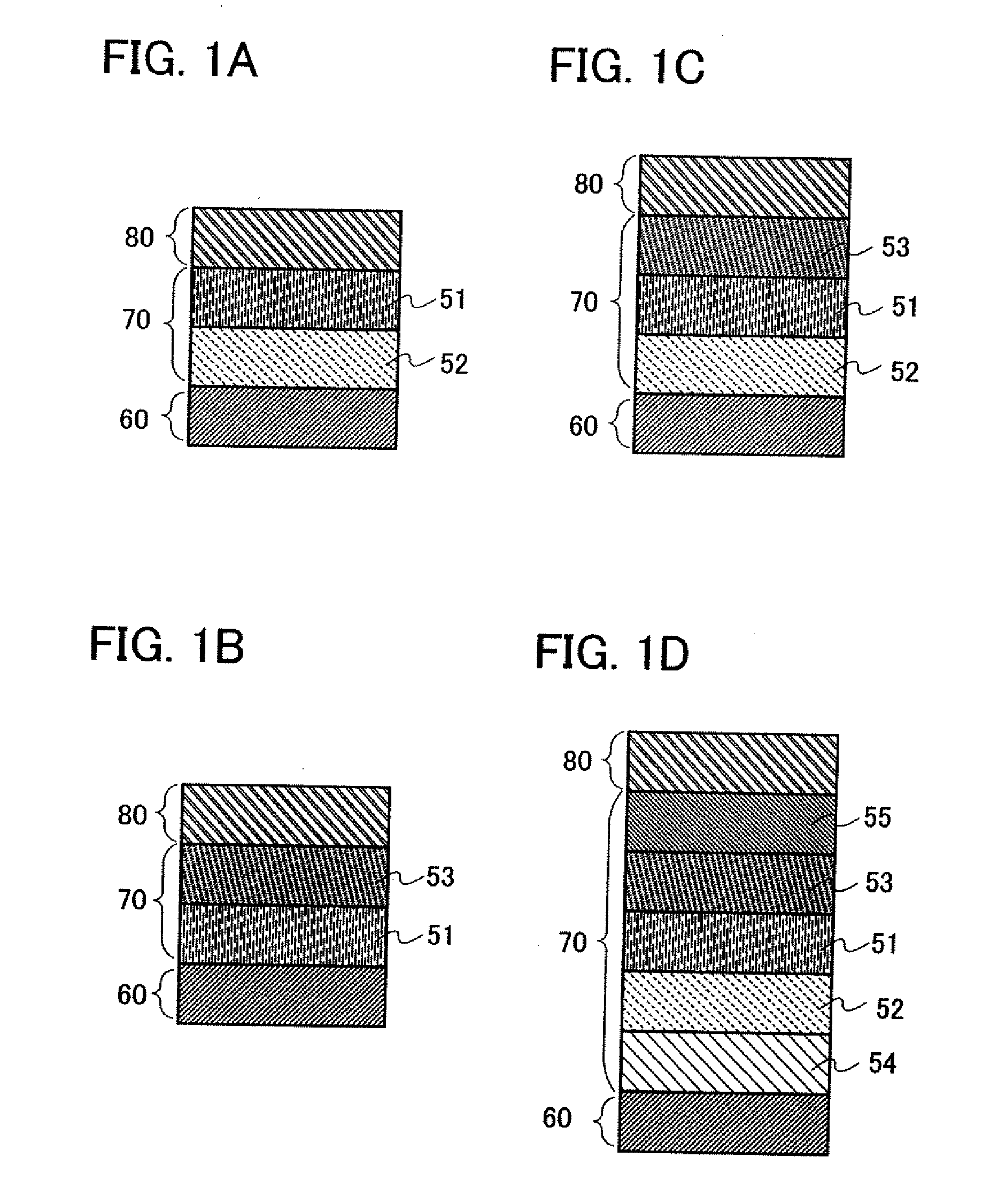
[0052]A light-emitting element in this embodiment mode will be explained in detail with reference to FIGS. 1A to 1D and FIGS. 2A to 2D.

[0053]The light-emitting element of the present invention includes an EL layer that has a stacked structure including a light-emitting layer containing an organic compound and a functional layer having a separate function between a pair of electrode layers. According to an aspect of the present invention, a mixed-valence compound is contained in a functional layer in a light-emitting element that includes an EL layer in which a light-emitting layer containing an organic compound and the functional layer are stacked.

[0054]A light emission mechanism is said to be as follows: by applying voltage to a pair of electrodes with an EL layer interposed therebetween, electrons injected from a cathode and holes injected from an anode (hereinafter, electrons or holes are also referred to as carriers) are recombined with each other in an emission center of a ligh...

embodiment mode 2

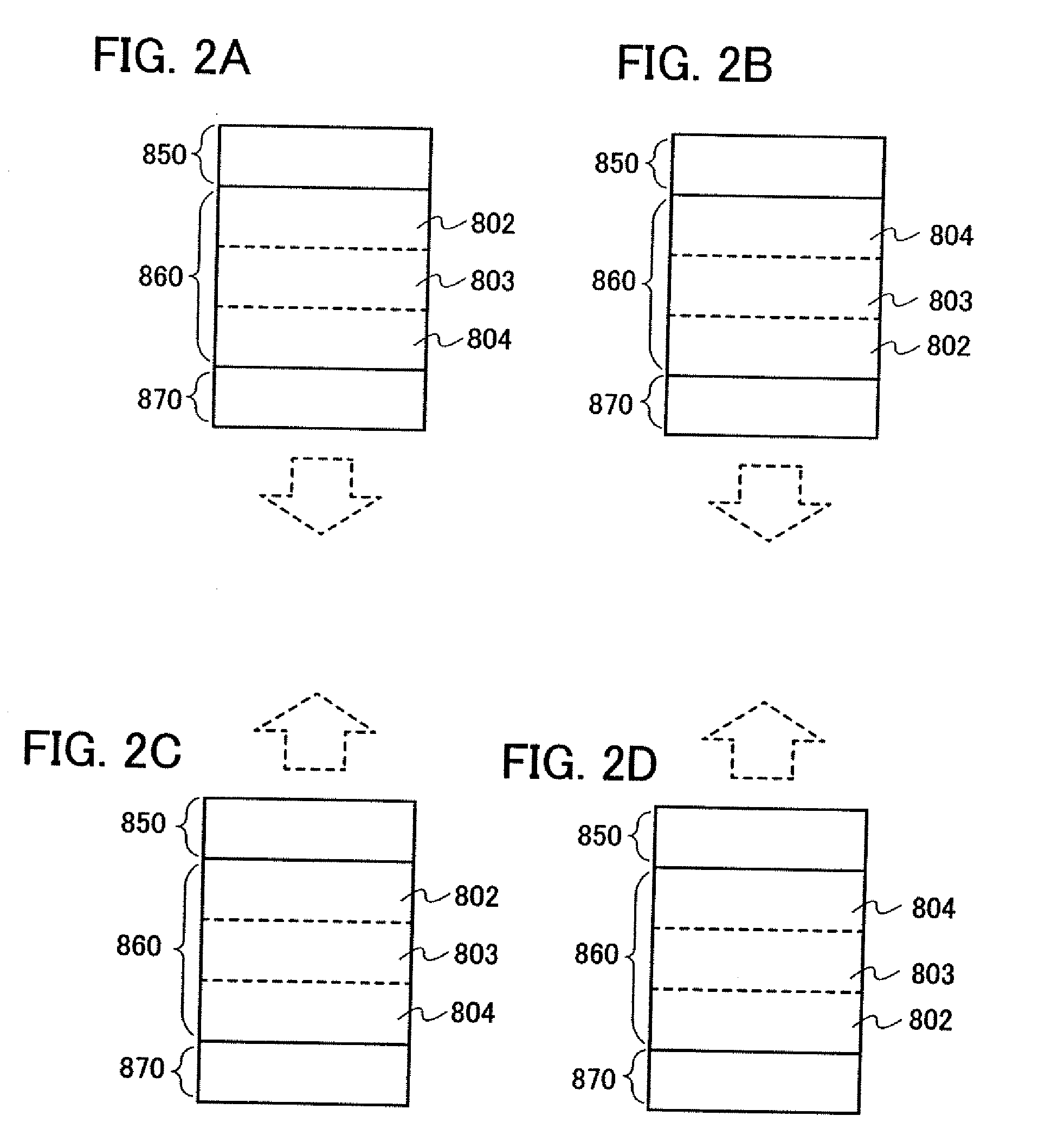
[0113]In this embodiment mode, a mode of a light-emitting element in which a plurality of light-emitting units according to the present invention are stacked (this light-emitting element is also referred to as a stacked-type element) will be explained with reference to FIG. 20. This light-emitting element is a light-emitting element including a plurality of light-emitting units between a first electrode layer and a second electrode layer.

[0114]In FIG. 20, a first light-emitting unit 511 and a second light-emitting unit 512 are stacked between a first electrode layer 501 and a second electrode layer 502. The first electrode layer 501 and the second electrode layer 502 can be similar to the electrode layers shown in Embodiment Mode 1. The first light-emitting unit 511 and the second light-emitting unit 512 may have either the same structure or a different structure, which may be similar to those shown in Embodiment Mode 1. Accordingly, a structure may be employed in which a mixed-vale...

embodiment mode 3

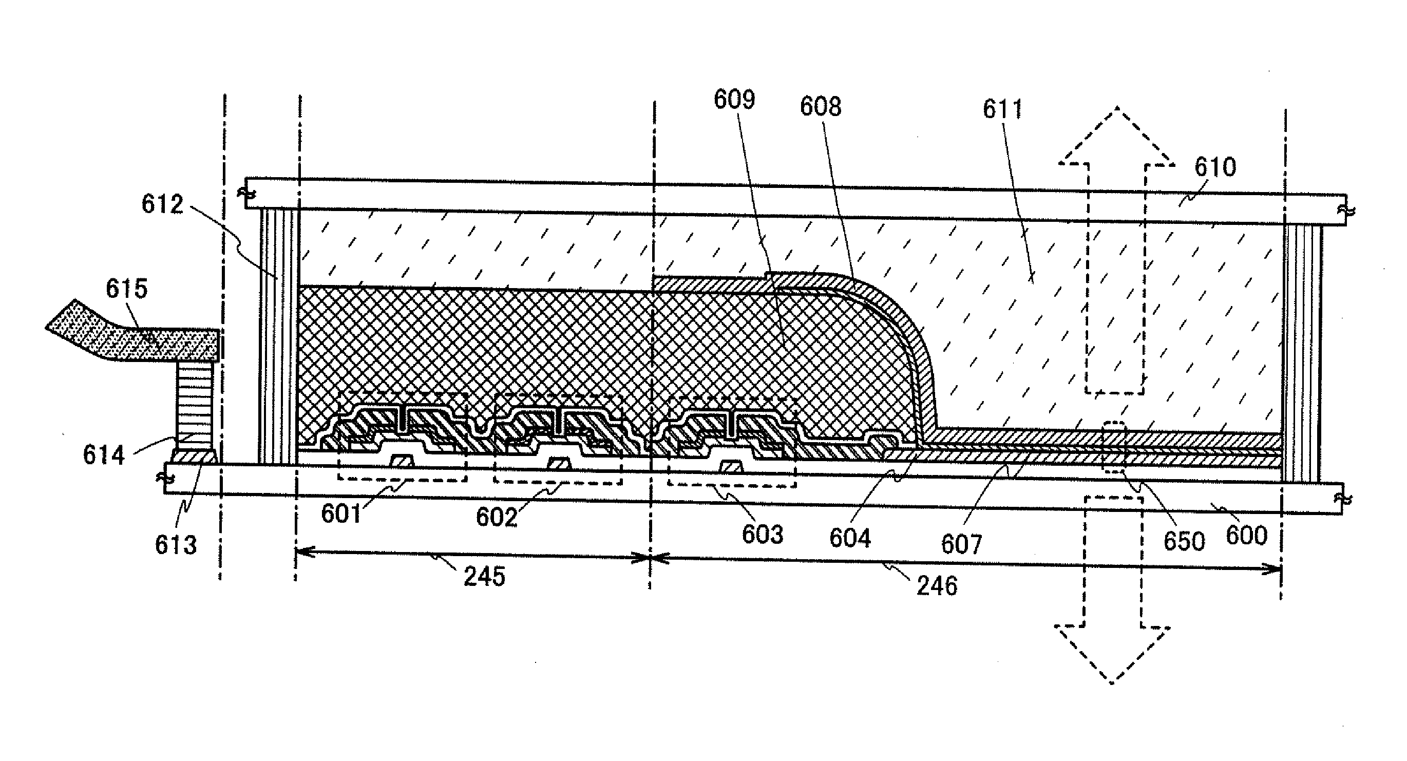
[0120]This embodiment mode will explain a structural example of a light-emitting device including the light-emitting element of the present invention with reference to drawings. More specifically, the case where a structure of a display device is a passive matrix type will be described.

[0121]The light-emitting device includes first electrode layers 751a, 751b, and 751c extending in a first direction; an EL layer 752 provided to cover the first electrode layers 751a, 751b, and 751c; and second electrode layers 753a, 753b, and 753c extending in a second direction perpendicular to the first direction (see FIG. 4A). The EL layer 752 has a stacked structure including a light-emitting layer containing an organic compound and a functional layer containing a mixed-valence compound. The EL layer 752 is provided between the first electrode layers 751a, 751b, and 751c and the second electrode layers 753a, 753b, and 753c. In addition, an insulating layer 754 functioning as a protective film is ...


PUM


Abstract

An object is to provide a highly functional and reliable light-emitting element and light-emitting device with lower power consumption and high emission efficiency. The light-emitting element has an EL layer that has a stacked structure including a light-emitting element containing an organic compound and a functional layer having separate functions between a pair of electrode layers. In the light-emitting element including the functional layer and the light-emitting element containing an organic compound, a mixed-valence compound is contained in the functional layers. When an element in a compound has a plurality of valences, this element is in a state that is referred to as a mixed-valence state and this compound is referred to as a mixed-valence compound.

Description

TECHNICAL FIELD[0001]The present invention relates to light-emitting elements and light-emitting devices.BACKGROUND ART[0002]As for organic compounds, there are a wider variety of materials and more possibilities to synthesize materials having various functions depending on the molecular design, compared with inorganic compounds. Because of these advantages, photo electronics and electronics each of which uses functional organic materials have been attracting attention in recent years.[0003]As examples of electronic devices using organic compounds as functional organic materials, there are solar cells, light-emitting elements, organic transistors, and the like. These are devices taking advantage of electric properties and optical properties of such organic compounds. In particular, light-emitting elements (electroluminescent (hereinafter, also referred to as “EL”) elements) have been making remarkable development.[0004]Such light-emitting elements have a lot of material-dependant pr...

Claims


Application Information

Patent Timeline
Patent Type & Authority Applications(United States)
IPC IPC(8): H01J1/62
CPCH01L51/5278H01L51/5048H10K50/14H10K50/19
Inventor OHARA, HIROKI
Owner SEMICON ENERGY LAB CO LTD
Why Eureka
Try Eureka