

Transistor having an etch stop layer including a metal compound that is selectively formed over a metal gate, and method therefor
a technology of metal compound and etch stop layer, which is applied in the field of transistors, can solve the problems of inoperable transistors, potential contact hole misalignment or misregistration, and increase the risk of electrical contact shortings
- Summary
- Abstract
- Description
- Claims
- Application Information
AI Technical Summary
Benefits of technology
Problems solved by technology
Method used
Image

Examples
Embodiment Construction
[0017]In the following description, numerous specific details are set forth. However, it is understood that embodiments of the invention may be practiced without these specific details. In other instances, well-known circuits, structures and techniques have not been shown in detail in order not to obscure the understanding of this description.
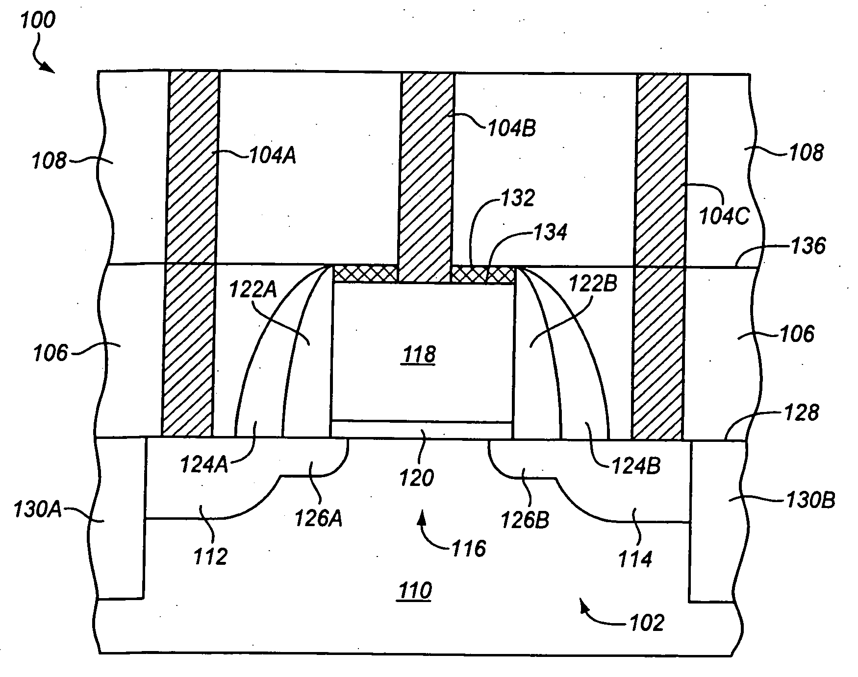
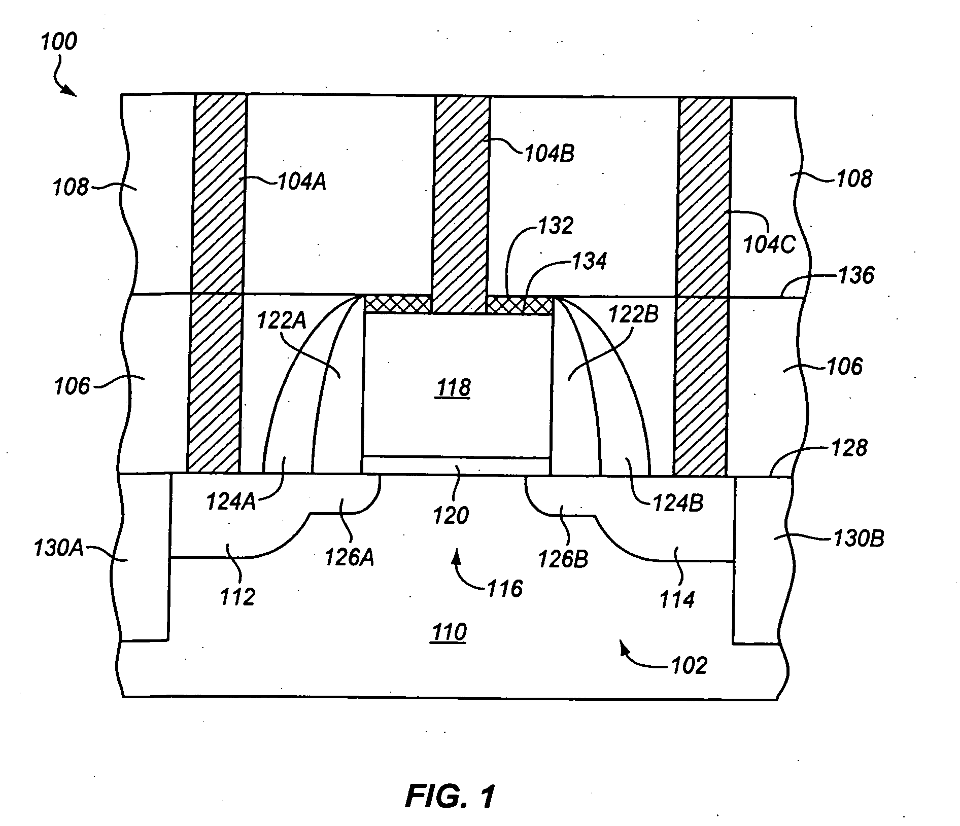
[0018]FIG. 1 is a cross-sectional side view of a microelectronic device 100, according to one or more embodiments of the invention. The microelectronic device includes a transistor 102 and electrical contacts 104A, 104B, 104C through insulating layers 106, 108 to the transistor.
[0019]The transistor represents one example of a suitable transistor. The transistor includes a source region 112 of a substrate 110, a drain region 114 of the substrate, and a channel region 116 of the substrate defined between the source and drain regions. The transistor also includes a metal gate 118 over the channel region, and a gate insulator or dielectric 120 disp...
PUM
| Property | Measurement | Unit |
|---|---|---|
| thickness | aaaaa | aaaaa |
| distance | aaaaa | aaaaa |
| thickness | aaaaa | aaaaa |
Abstract
Description
Claims
Application Information