Scalable Embedded DRAM Array

a dram array and embedded technology, applied in the field of dynamic random accessible memory, can solve the problems of difficult to maintain a constant storage capacitance complicate the process required to fabricate dram cells,

Active Publication Date: 2008-07-03
MOSYS INC
View PDF61 Cites 6 Cited by
  • Summary
  • Abstract
  • Description
  • Claims
  • Application Information

AI Technical Summary

Problems solved by technology

However, it is difficult to maintain a constant storage capacitance CC across advancing processes.
However, increasing these vertical dimensions such that a constant capacitance is maintained across advancing processes further complicates the process required to fabricate DRAM cell 300.
However, increasing this depth such that a constant capacitance is maintained across advancing processes further complicates the process required to fabricate DRAM cell 400.
In general, the higher the stack or the deeper the trench, the more complicated the processing steps required to form the cell capacitor.
However, the use of non-standard dielectric materials adds cost and complexity to the associated process.

Method used


Image

  • Scalable Embedded DRAM Array
  • Scalable Embedded DRAM Array
  • Scalable Embedded DRAM Array

Examples


Embodiment Construction

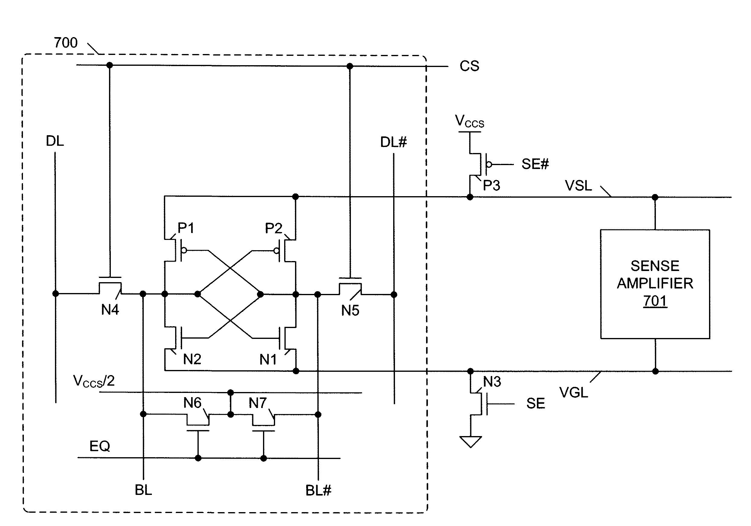
[0039]In accordance with the present invention, the sensing voltage VS of embedded DRAM arrays in advancing processes is maintained at a constant level by applying the same supply voltage to the DRAM sense amplifiers across these advancing processes. This is in contrast with the above-described prior art, in which the sensing voltage VS of embedded DRAM arrays in advancing processes is maintained at a constant level by maintaining a constant cell capacitance CC across these advancing processes.

[0040]In the present specification, the constant supply voltage applied to the sense amplifiers across advancing processes is designated VCCS. Although the sense amplifier supply voltage VCCS remains constant, the VCC supply voltage continues to be reduced across advancing processes. The VCC supply voltage is still used to supply the rest of the on-chip circuitry (e.g., embedded logic circuits).

[0041]Substituting the constant sense amplifier supply voltage VCCS into equation (2) provides the f...


PUM


Abstract

A method and apparatus for scaling an embedded DRAM array from a first process to a second process, wherein the scaling involves reducing the linear dimensions of features by a constant scale factor. From the first process to the second process, DRAM cell capacitor layout area is reduced by the square of the scale factor, while cell capacitance is reduced by the scale factor. The voltage used to supply the logic transistors is scaled down from the first process to the second process. However, the voltage used to supply the sense amplifiers remains constant in both processes. Thus, in an embedded DRAM array of the second process, sense amplifiers are supplied by a greater voltage than the logic transistors. This allows the sensing voltage of DRAM cells to be maintained from one process generation to another, while allowing memory size to scale with the square of the process scale factor.

Description

RELATED APPLICATIONS[0001]The present application is a divisional of U.S. patent application Ser. No. 11 / 534,506 by Wingyu Leung, entitled “Scalable Embedded DRAM Array”, which is a continuation-in-part of U.S. patent application Ser. No. 11 / 166,856 by Wingyu Leung, entitled “Word Line Driver For DRAM Embedded in A Logic Process”.[0002]The present application is also related to U.S. Pat. No. 6,028,804, by Wingyu Leung, entitled “Method and Apparatus for 1-T SRAM Compatible Memory”, U.S. Pat. No. 6,573,548 B2 by Wingyu Leung and Fu-Chieh Hsu, entitled “DRAM cell having a capacitor structure fabricated partially in a cavity and method for operating the same”, U.S. Pat. No. 6,147,914 by Wingyu Leung and Fu-Chieh Hsu, entitled “On-chip word line voltage generation for DRAM embedded in Logic Process”, and U.S. Pat. No. 6,075,720 by Wingyu Leung and Fu-Chieh Hsu, entitled “Memory cell for DRAM embedded in Logic”. As described in more detail below, these patent applications are incorporate...

Claims


Application Information

Patent Timeline
Patent Type & Authority Applications(United States)
IPC IPC(8): G11C7/02
CPCG11C8/08H01L27/10897G11C2207/104G11C11/4085H10B12/50G11C11/40G11C5/14G11C7/06
Inventor LEUNG, WINGYU
Owner MOSYS INC
Why Eureka
Try Eureka