Page by page ecc variation in a memory device

a memory device and page by page technology, applied in the field of nonvolatile memory, can solve the problems of erroneous reading of data stored failure of attempted data read, etc., and achieve the effect of higher data integrity

Active Publication Date: 2008-07-03
SANDISK TECH LLC
View PDF2 Cites 25 Cited by
  • Summary
  • Abstract
  • Description
  • Claims
  • Application Information

AI Technical Summary

Benefits of technology

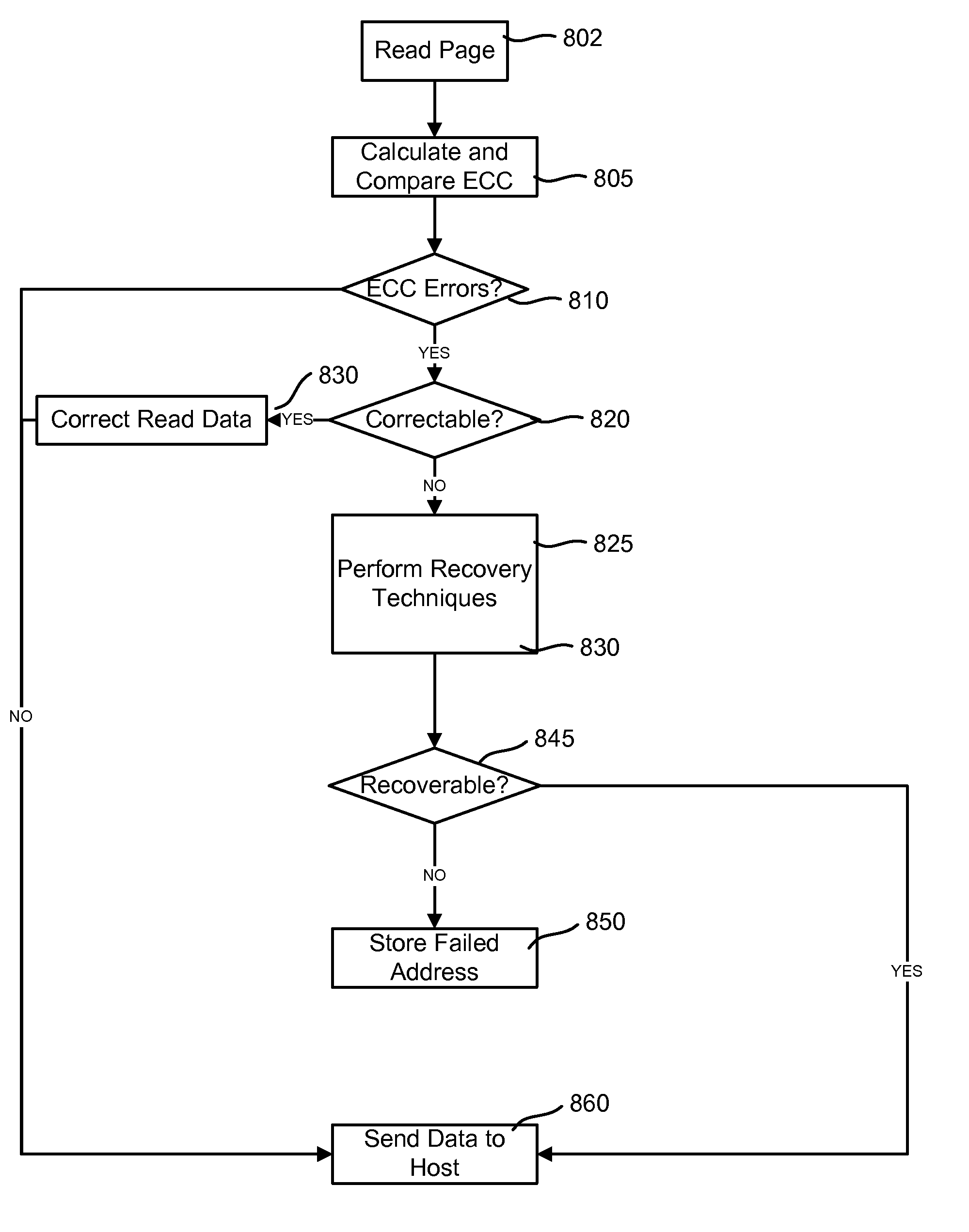
[0011]In one aspect, a data structure for a memory device is provided. The device includes an array having a plurality of rows of storage elements divided into logical units composed of a plurality of data structures. The data sector includes user data and user attribute data. The user attribute data including error correction coding (ECC) for the user data and the user attribute data including block level information. The data sector provided in one of the plurality of rows having a higher degree of data integrity than others of said plurality of rows.
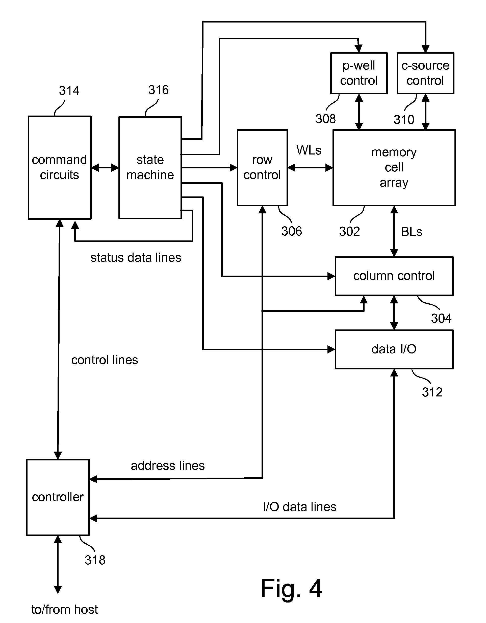
[0012]In a second aspect, a memory device includes an array of multi-state storage elements, rows of said data elements comprising logical pages and a controller. The controller is coupled to the array and performs programming operations including programming user data into a page of said block having a higher degree of data integrity than others of said plurality of pages. The controller further programs data attribute information including error correction code (ECC) in a portion of a data sector of the page and stores block level data attributes in a second portion of the data sector, said second portion of the data sector being a location occupied by ECC information in said others of said pages.

Problems solved by technology

The coupling from adjacent memory cells can shift the apparent charge level being read a sufficient amount to lead to an erroneous reading of the data stored.
One or a few erroneous bits of data within a sector of data can often be corrected by use of the ECC but the existence of more errors renders the attempted data read to fail.
Thus, the existence of bits that are read incorrectly because of close field coupling with adjacent memory cells can cause an attempted data read to fail.

Method used


Image

  • Page by page ecc variation in a memory device
  • Page by page ecc variation in a memory device
  • Page by page ecc variation in a memory device

Examples


Embodiment Construction

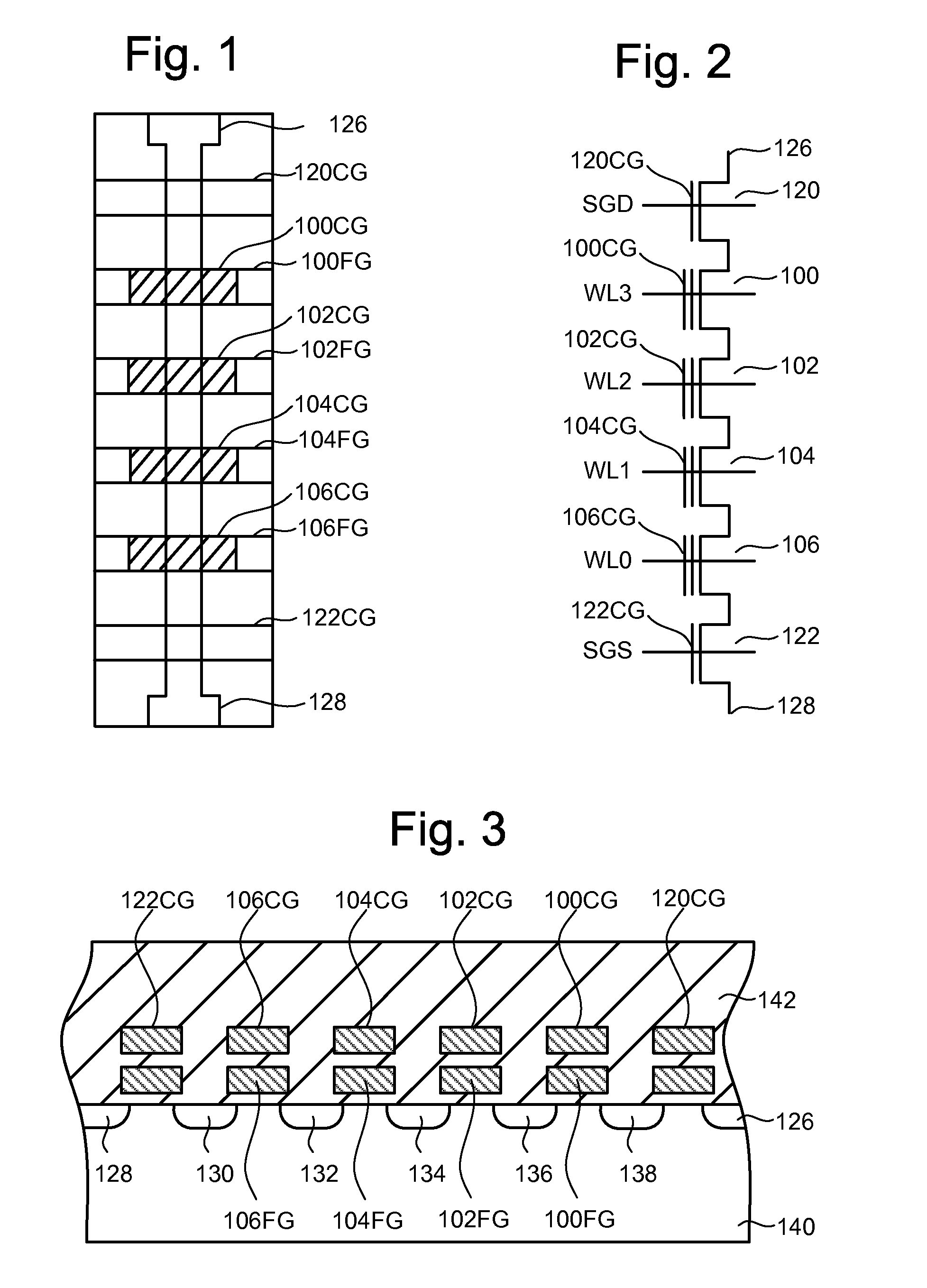
[0024]Technology is disclosed herein for optimizing the use of overhead in pages of data which have greater data reliability. Greater reliability can result from being subject to little or less floating-gate to floating-gate coupling or a row being designed to have greater spacing and / or greater line width (and hence greater channel lengths) from adjacent rows. User data is stored along with overhead information associated with overhead information concerning a logical block of data comprised of a set of pages. Such overhead information includes block hot count, compressed block hot count, a block rewrite flag, and logical to physical translation information. This overhead information can be stored in a portion of a page normally used for ECC information, since less ECC capability is required due to the greater reliability of the page.

[0025]The technology will be described with respect to one example of a flash memory system using a NAND structure which includes arranging multiple t...


PUM


Abstract

A data structure for a memory device is provided. The device includes an array having a plurality of rows of storage elements divided into logical units composed of a plurality of data structures. The data structure includes a data sector including user data and user attribute data. The user attribute data includes error correction coding (ECC) for the user data. The user attribute data includes information for other sectors in the logical unit. The data sector is provided in one of the plurality of rows having a higher degree of data integrity than others of said plurality of rows.

Description

BACKGROUND OF THE INVENTION[0001]1. Field of the Invention[0002]The present invention relates to technology for non-volatile memory.[0003]2. Description of the Related Art[0004]Semiconductor memory devices have become more popular for use in various electronic devices. For example, non-volatile semiconductor memory is used in cellular telephones, digital cameras, personal digital assistants, mobile computing devices, non-mobile computing devices and other devices.[0005]Electrical Erasable Programmable Read Only Memory (EEPROM) and flash memory utilize a floating gate that is positioned above and insulated from a channel region in a semiconductor substrate. The floating gate is positioned between the source and drain regions. A control gate is provided over and insulated from the floating gate. The threshold voltage of the transistor is controlled by the amount of charge that is retained on the floating gate. That is, the minimum amount of voltage that must be applied to the control ...

Claims


Application Information

Patent Timeline
Patent Type & Authority Applications(United States)
IPC IPC(8): G06F11/16
CPCG06F11/1072
Inventor MOKHLESI, NIMA
Owner SANDISK TECH LLC
Why Eureka
Try Eureka