Connection structure of flexible substrate

a technology of connecting structure and flexible substrate, which is applied in the direction of magnetic bodies, manufacturing tools, cores/yokes, etc., can solve the problems of increasing the outside dimension and the figure increase, and achieve the effect of reducing the outside dimension of the counterpart substrate 1 and forming easily

Inactive Publication Date: 2008-07-10
FUNAI ELECTRIC CO LTD
View PDF6 Cites 0 Cited by
  • Summary
  • Abstract
  • Description
  • Claims
  • Application Information

AI Technical Summary

Benefits of technology

[0012]Hence, the present inventor focused his attention on the facts that the width of the space S1 between the two spaced-apart solder lands 21 and 22 shown in FIG. 8 has a dimension appropriate to the width between the solder lands 61 and 62 on the flexible substrate 5 shown in FIG. 9 and that the space S1 is a dead space in the connection structure shown in FIG. 6 unavailable for mounting of electrical and electronic elements such as ICs and capacitors, and considered that reducing the area of the space S1 could reduce the outside dimension of the counterpart substrate 1 accordingly.
[0013]Under such circumstances, the present inventor has worked out a connection structure of a flexible substrate whereby the width dimension W and therefore the outside dimension of the counterpart substrate 1 shown in FIG. 6 can be reduced by reducing the width W1 between the two spaced-apart solder lands 21 and 22 on the counterpart substrate 1, that is, reducing the width of the space S1 in FIG. 8 without changing the density of many circuit patterns on the flexible substrate 5 in FIG. 9.
[0014]Accordingly, it is an object of the present invention to provide a connection structure of a flexible substrate whereby the outside dimension of a counterpart substrate can be reduced by reducing the area of a dead space on the counterpart substrate due to being covered with a flexible substrate when the flexible substrate is connected by soldering to the counterpart substrate.

Problems solved by technology

Meanwhile, it is known that PCBs like the counterpart substrate 1 shown in FIG. 6 and other figures increase in cost with an increase in the outside dimension thereof.

Method used


Image

  • Connection structure of flexible substrate
  • Connection structure of flexible substrate
  • Connection structure of flexible substrate

Examples


Embodiment Construction

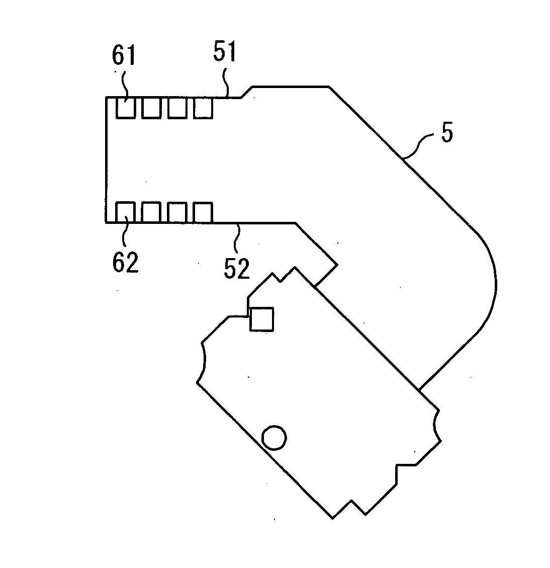
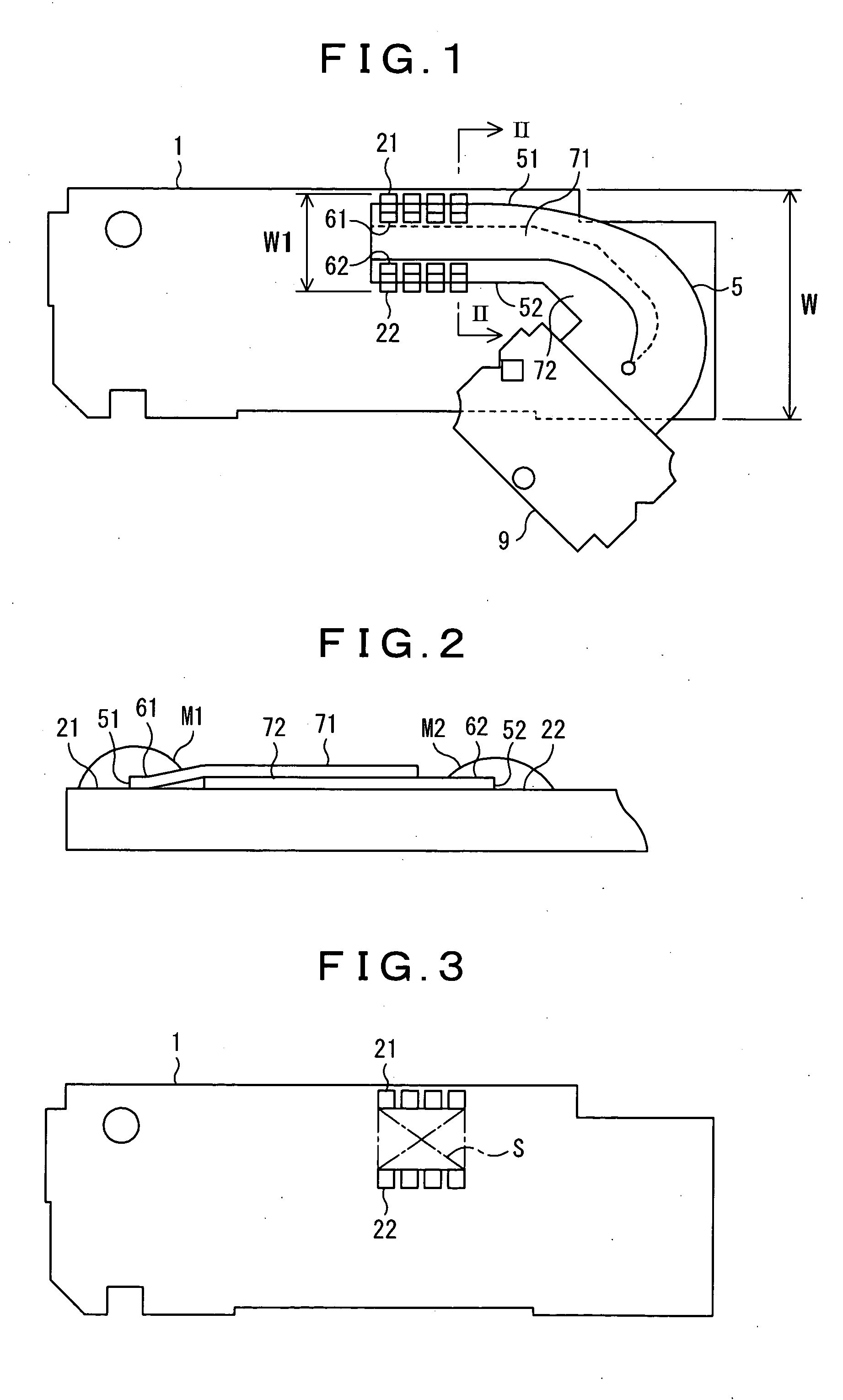
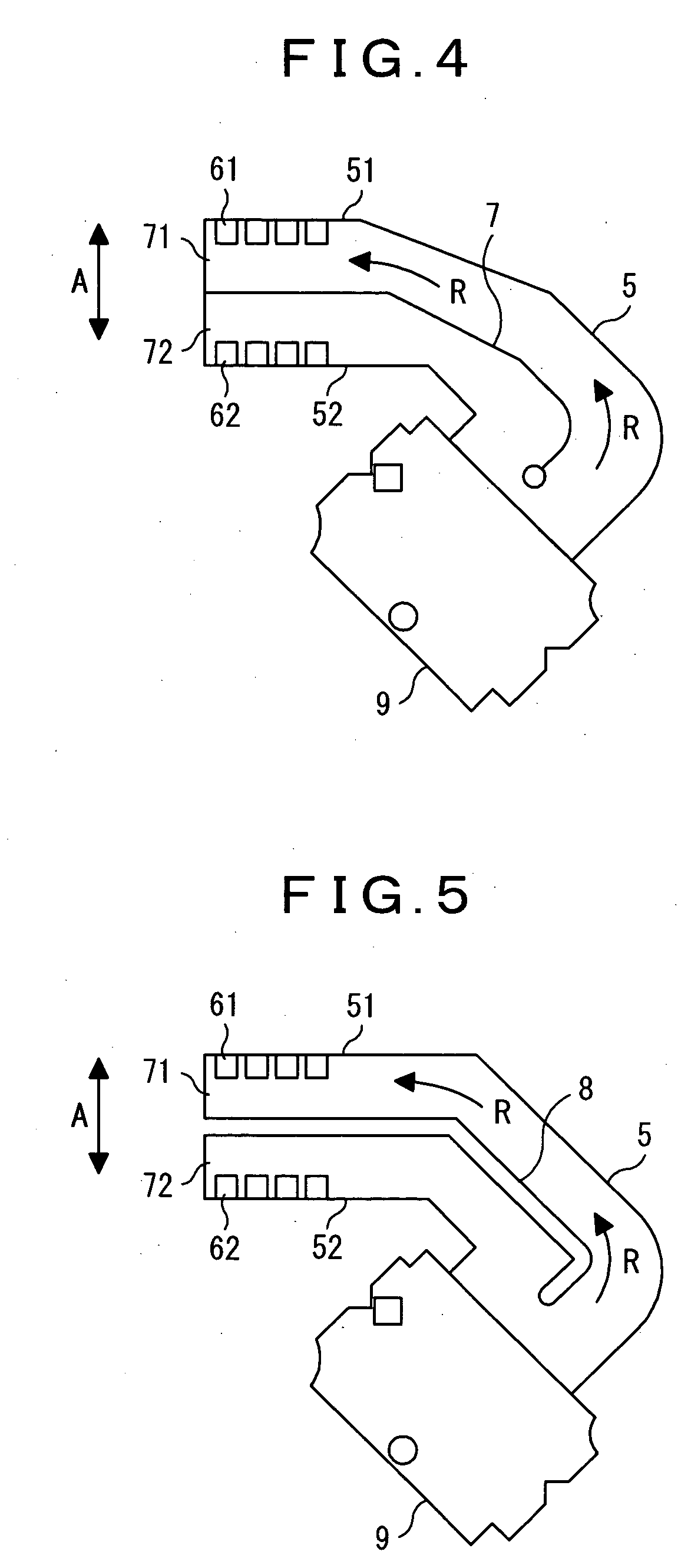
[0031]FIG. 1 is a plan view of a connection structure of a flexible substrate according to an embodiment, and FIG. 2 is an illustrative enlarged cross-sectional view along the arrows II-II in FIG. 1. Further, FIG. 3 is a schematic plan view of a counterpart substrate 1 according to the embodiment, and FIG. 4 is a schematic plan view of a flexible substrate 5 according to the embodiment.

[0032]In the present embodiment, the counterpart substrate 1 is used as a control substrate for an optical pickup for optically processing a disk as a recording medium to be used in the DVD drive, and the base end portion of the flexible substrate 5 is connected to an optical component 9 such as a photodetector.

[0033]As shown in FIG. 1 or 2, the present embodiment has a basic configuration in which solder lands 61 and 62 formed in both of the lateral edge portions 51 and 52 of the flexible substrate 5 that has many parallel circuit patterns arranged thereon are connected by soldering M1 and M2, respec...


PUM

PropertyMeasurementUnit
flexibleaaaaaaaaaa
sizeaaaaaaaaaa
flexibilityaaaaaaaaaa

Abstract

In the case of connecting a flexible substrate to a counterpart substrate by soldering, the area of a dead space on the counterpart substrate due to being covered with the flexible substrate is reduced to reduce the outside dimension of the counterpart substrate. Solder lands 61 and 62 on the flexible substrate 5 are soldered to solder lands 21 and 22 on the counterpart substrate 1. The flexible substrate 5 is divided into two branching pieces 71 and 72 by an incision 7 or a slit 8 formed in such a manner as to extend from an intermediate part in the arrangement direction R of circuit patterns to the leading end of the flexible substrate. The space between the solder lands 61 and 62 on the respective pieces 71 and 72 is made equal to the space between the two spaced-apart solder lands 21 and 22 on the counterpart substrate 1 by placing the pieces 71 and 72 formed by dividing the flexible substrate 5 on one another.

Description

BACKGROUND OF THE INVENTION[0001]1. Field of the Invention[0002]The present invention relates to a connection structure of a flexible substrate, in particular, with measures taken therein to narrow the space between two spaced-apart solder lands formed on a counterpart substrate and thereby to facilitate reducing the size of the counterpart substrate in the case of connecting solder lands formed in both of the lateral edge portions of the flexible substrate to the two respective spaced-apart solder lands on the counterpart substrate by soldering.[0003]2. Description of the Related Art[0004]FIG. 6 is a plan view showing a connection structure of a flexible substrate according to a conventional example, and FIG. 7 is an illustrative enlarged cross-sectional view along the arrows VII-VII in FIG. 6. Further, FIG. 8 is a schematic plan view showing a counterpart substrate 1 according to the conventional example, and FIG. 9 is a schematic plan view showing a flexible substrate 5 according...

Claims


Application Information

Patent Timeline
Patent Type & Authority Applications(United States)
IPC IPC(8): B32B3/10
CPCH05K1/147Y10T428/12H05K2201/053H05K3/363
Inventor NISHIDATE, TETSUO
Owner FUNAI ELECTRIC CO LTD
Why Eureka
Try Eureka