Memory Controller, Nonvolatile Storage Device, Nonvolatile Storage System, and Memory Control Method

Active Publication Date: 2008-07-10
PANASONIC CORP
View PDF6 Cites 36 Cited by
  • Summary
  • Abstract
  • Description
  • Claims
  • Application Information

AI Technical Summary

Benefits of technology

[0024]According to the invention, time required for creating an address management table at the time of initialization can be shorte

Problems solved by technology

However, in the semiconductor memory card having a memory space of large capacity, a much time is taken for reading out distributed management information of the whole memory space at the time of initialization.
As a result, it may exceed the upper limit of standard initialization time in the semiconductor memory card, or cause other

Method used


Image

  • Memory Controller, Nonvolatile Storage Device, Nonvolatile Storage System, and Memory Control Method
  • Memory Controller, Nonvolatile Storage Device, Nonvolatile Storage System, and Memory Control Method
  • Memory Controller, Nonvolatile Storage Device, Nonvolatile Storage System, and Memory Control Method

Examples


first embodiment

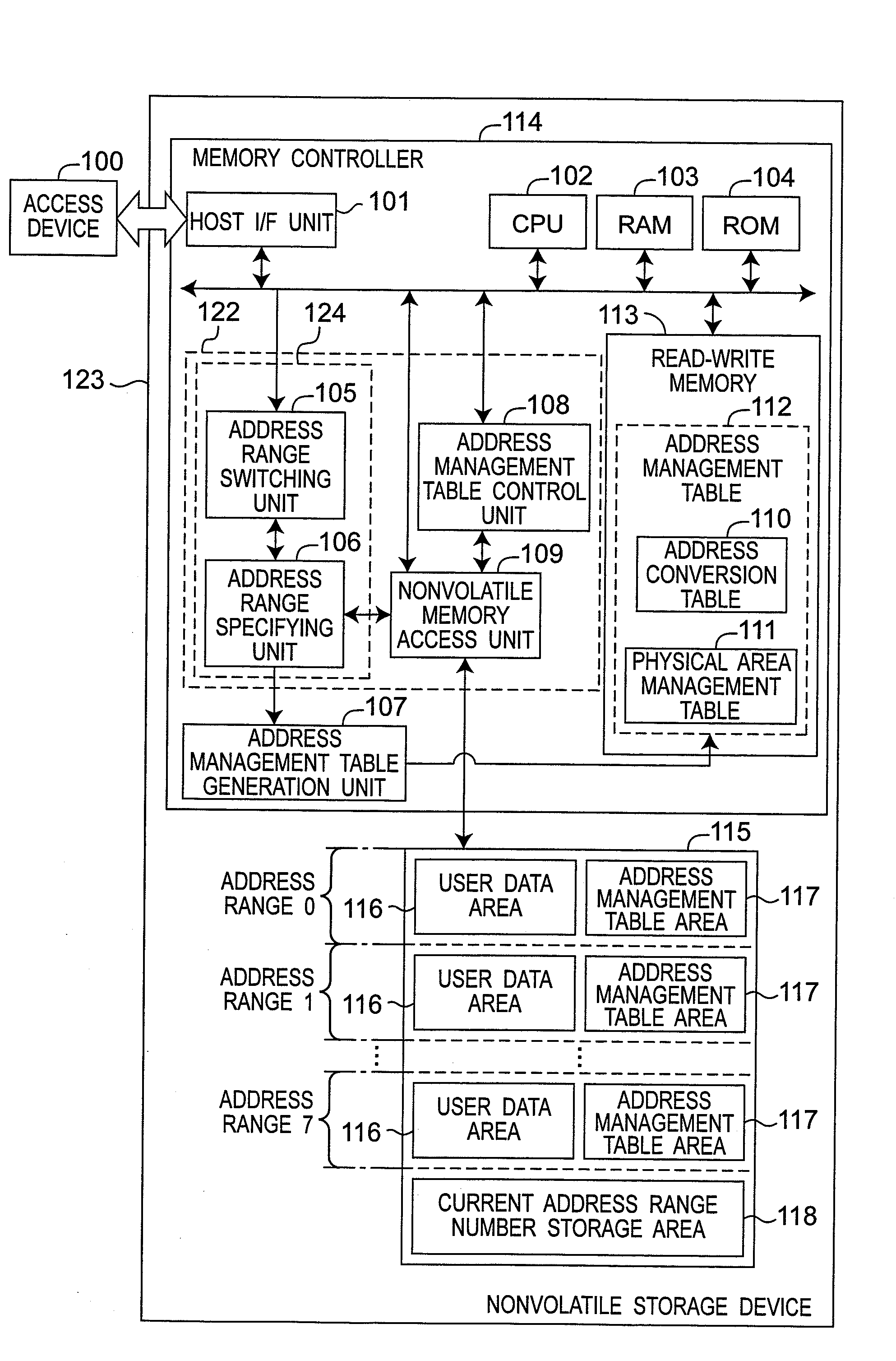
[0076]FIG. 1 shows a configuration of nonvolatile storage system in the embodiment. The nonvolatile storage system in the embodiment includes an access device 100, and a nonvolatile storage device 123 that operates according to a read or write command of user data (or “data”) sent from the access device 100.

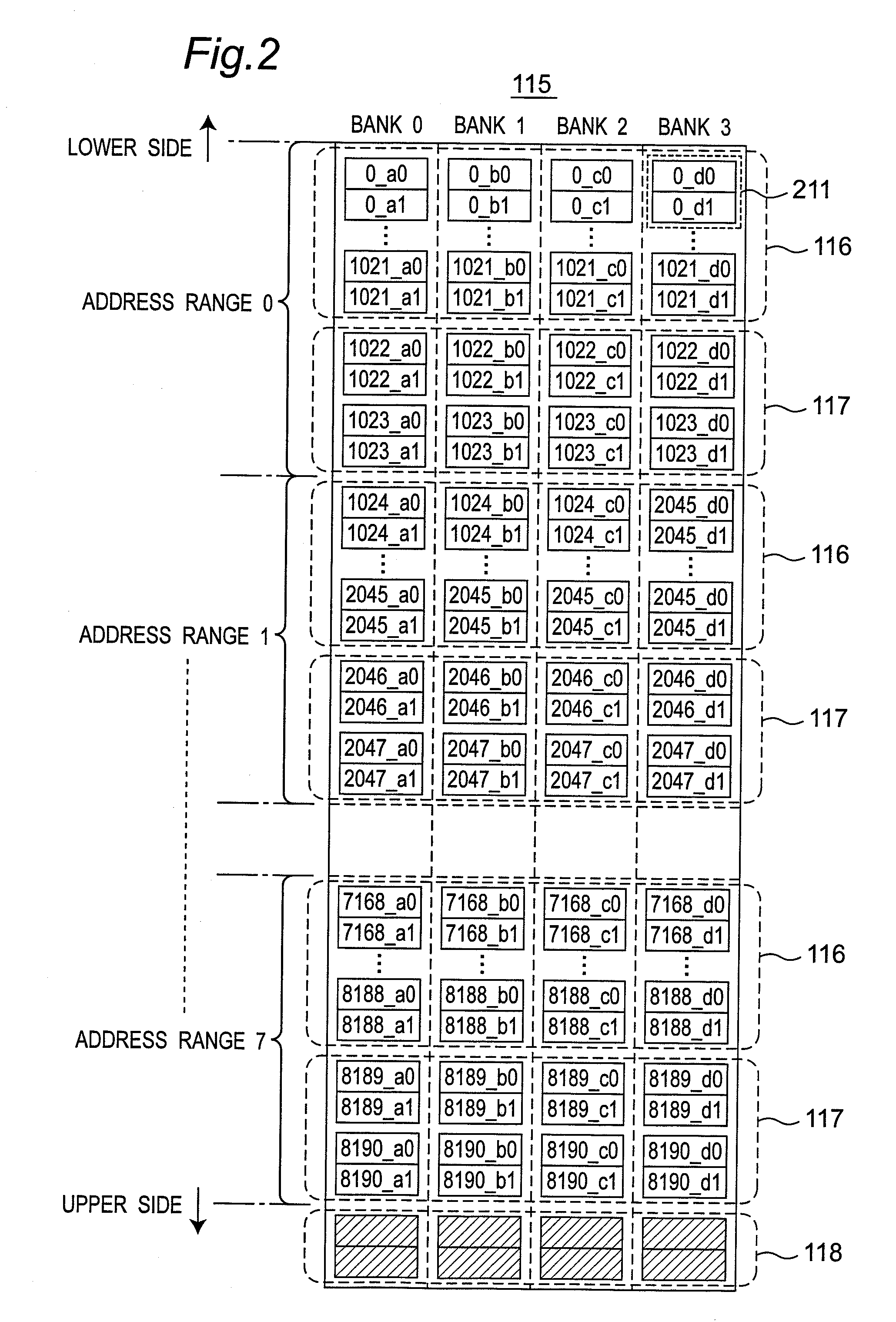
[0077]The nonvolatile storage device 123 includes a nonvolatile memory 115 that stores the data transferred from the access device 100, and a memory controller 114 that controls the nonvolatile memory 115 based on a read or write command and a logical address sent from the access device 100. The storage area of the nonvolatile memory 115 is divided into a plurality of address ranges.

[Internal Configuration of Memory Controller]

[0078]The memory controller 114 has a host interface unit (hereafter, referred to as “host I / F unit”) 101, a RAM 103 for work, a ROM 104 storing a program, and a CPU 102 that controls the whole memory controller 114 by using the work RAM 103 and the program...

second embodiment

[0142]FIG. 11 is a block diagram of nonvolatile storage system in the second embodiment of the invention. The nonvolatile storage system in the embodiment is similar to the first embodiment, except for the size of address range of nonvolatile memory 1115, and the generating method of address management table 1112 at the time of initialization.

[0143]The nonvolatile storage system of the embodiment includes an access device 100 and a nonvolatile storage device 123 operating based on the read or write command of data sent from the access device 100.

[0144]The nonvolatile storage device 123 includes a nonvolatile memory 1115 that stores the data transferred from the access device 100, and a memory controller 114 that controls the nonvolatile memory 1115 based on the read or write command and logical address sent from the access device 100. The storage area of the nonvolatile memory 1115 includes a plurality of address ranges.

[Internal Configuration of Memory Controller]

[0145]The memory c...


PUM


Abstract

The invention presents a memory controller capable of shortening the creation time of address management table at the time of initialization of memory card, while avoiding decline of access speed due to process of writing back the address management table in normal operation.
The memory controller 114 includes a read-write memory 113 for temporarily storing the address management table 112, a memory control unit 122 for writing, in a nonvolatile memory 115, an address management table temporarily stored in the read-write memory and address range specifying information for specifying the changeover destination address range, when the physical block of data writing destination is changed over from a certain address range to other address range, and an address management table generation unit 107 for reading out the distributed management information used for managing the state of physical block included in the address range specified based on the address range specifying information at the time of initialization, and generating the address management table 112 based on the distributed management information being read out.

Description

TECHNICAL FIELD[0001]The invention relates to a nonvolatile storage device such as a semiconductor memory card having a flash memory as a main storage memory, a memory controller incorporated therein, a nonvolatile storage system including the nonvolatile storage device and an access device, and a memory control method.BACKGROUND ART[0002]A nonvolatile storage device including a re-writable nonvolatile memory is increasing in its demand mainly for use in semiconductor memory card. A nonvolatile storage system using the semiconductor memory card is also increasing in its demand mainly for use in digital still camera and personal computer.[0003]A practical semiconductor memory card usually includes a flash memory as a nonvolatile memory and a controller LSI as its control circuit, inside. Recently, in the trend of larger capacity of semiconductor memory card, the nonvolatile memory chip is also increased in capacity by multiple-value configuration. Owing to the progress in mounting te...

Claims


Application Information

Patent Timeline
IPC IPC(8): G06F12/02G06F12/00
CPCG06F2212/7201G06F12/0246
Inventor KUNIMUNE, DAISUKENAKANISHI, MASAHIROINOUE, MANABUIZUMI, TOMOAKIKASAHARA, TETSUSHITAMURA, KAZUAKIMATSUNO, KIMINORI
Owner PANASONIC CORP
Why Eureka
Try Eureka