Electroluminescent display

a technology of el and el, applied in the direction of discharge tube/lamp details, discharge tube luminescnet screens, transportation and packaging, etc., can solve the problems of soft failure phenomenon, insufficient shielding of internal elements, and reduced thickness of conventional el displays

Inactive Publication Date: 2008-07-17
SAMSUNG DISPLAY CO LTD
View PDF14 Cites 27 Cited by
  • Summary
  • Abstract
  • Description
  • Claims
  • Application Information

AI Technical Summary

Benefits of technology

[0008]It is therefore a feature of an embodiment of the present invention to provide an EL display havi

Problems solved by technology

However, a reduced thickness of the conventional EL display, e.g., about 1 mm to about 2 mm, may be insufficient to shield internal elements thereof, e.g., the LED, from external electrostatic impacts.
For example, a strong flow of an electrostatic discharge, e.g., voltage of about several thousands of volts or several

Method used


Image

  • Electroluminescent display
  • Electroluminescent display
  • Electroluminescent display

Examples


Embodiment Construction

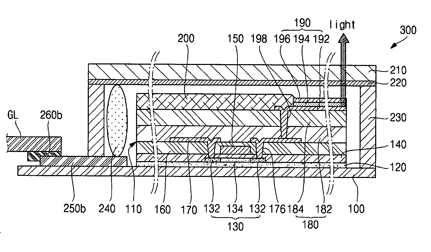
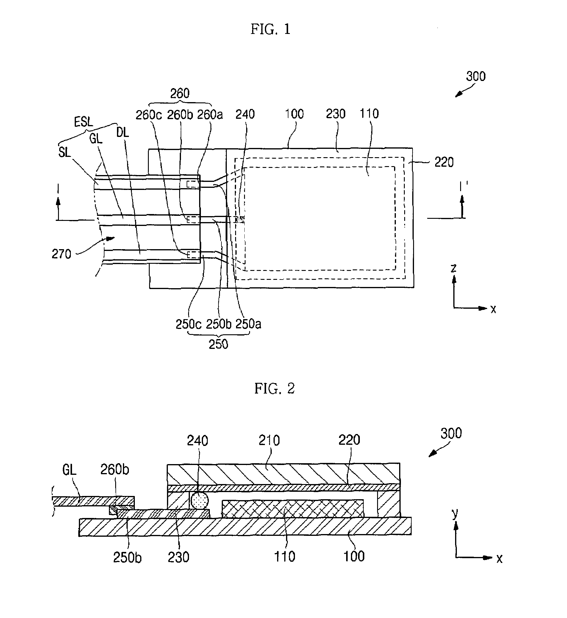
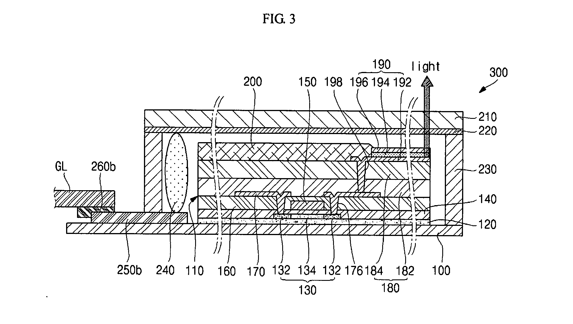
[0025]Korean Patent Application No. 10-2007-0004438 filed on Jan. 15, 2007 in the Korean Intellectual Property Office and entitled: “Organic Electroluminescence Display,” is incorporated by reference herein in its entirety.

[0026]The present invention will now be described more fully hereinafter with reference to the accompanying drawings, in which exemplary embodiments of the invention are illustrated. The invention may, however, be embodied in different forms and should not be construed as limited to the embodiments set forth herein. Rather, these embodiments are provided so that this disclosure will be thorough and complete, and will fully convey the scope of the invention to those skilled in the art.

[0027]In the figures, the dimensions of layers and regions may be exaggerated for clarity of illustration. It will also be understood that when a layer or element is referred to as being “on” another layer or substrate, it can be directly on the other layer or substrate, or intervenin...


PUM


Abstract

An electroluminescent (EL) display includes a substrate, an EL pixel array with a light emitting diode (LED) on the substrate, a connector electrically coupled to the EL pixel array, an encapsulant on the substrate and surrounding the EL pixel array, an encapsulation substrate attached to the substrate, the EL pixel array enclosed between the encapsulation substrate and the substrate, and a conductive film electrically coupled to the connector, the conductive film being in communication either with the substrate or the encapsulation substrate.

Description

BACKGROUND OF THE INVENTION[0001]1. Field of the Invention[0002]Embodiments of the present invention relate to an electroluminescent (EL) display. More particularly, embodiments of the present invention relate to an EL display providing an improved protection to its internal components from external electrostatic discharge.[0003]2. Description of the Related Art[0004]Generally, an electroluminescent (EL) display is a flat panel display device employing a light emitting diode (LED) activated by combination of electrons and holes from a cathode and an anode, respectively, in a light emitting layer of the LED. In other words, the LED may include a light emitting layer between the anode and the cathode, so that applied voltage may trigger electron / hole flow from the cathode / anode into the light emitting layer to activate light emission. Such EL displays may be employed in mobile communication terminals, navigation devices, personal display assistances (PDAs), camcorders, and so forth.[0...

Claims


Application Information

Patent Timeline
IPC IPC(8): H01J1/62
CPCH01L27/3272H01L51/5237H01L27/3276H10K59/126H10K59/131H10K50/8423H10K50/8426H10K50/865A47K11/00E04H1/1216E03D7/00B60R15/04
Inventor KIM, MIHAECHOI, WOONGSIK
Owner SAMSUNG DISPLAY CO LTD
Why Eureka
Try Eureka