Image sensor module and the method of the same

a technology of image sensor and module, which is applied in the direction of radio frequency control devices, instruments, television systems, etc., can solve the problems of not meeting the demand of producing small chips with high density elements on the chip, requiring many expensive optical elements, and requiring rigid package techniques, etc., to achieve the effect of simple process and small footprin

Inactive Publication Date: 2008-07-24
ADVANCED CHIP ENG TECH
View PDF0 Cites 99 Cited by
  • Summary
  • Abstract
  • Description
  • Claims
  • Application Information

AI Technical Summary

Benefits of technology

[0008]The object of the present invention is to provide an image sensor module with PCB having cavi...

Problems solved by technology

This can require many expensive optical elements.
As a semiconductor become more complicated, the traditional package technique, for example lead frame package, flex package, rigid package technique, can't meet the demand of producing smaller chip with high density elements on the chip.
Because conventional package technologies have to d...

Method used


Image

  • Image sensor module and the method of the same
  • Image sensor module and the method of the same
  • Image sensor module and the method of the same

Examples


Embodiment Construction

[0021]The invention will now be described in greater detail with preferred embodiments of the invention and illustrations attached. Nevertheless, it should be recognized that the preferred embodiments of the invention is only for illustrating. Besides the preferred embodiment mentioned here, present invention can be practiced in a wide range of other embodiments besides those explicitly described, and the scope of the present invention is expressly not limited expect as specified in the accompanying Claims.

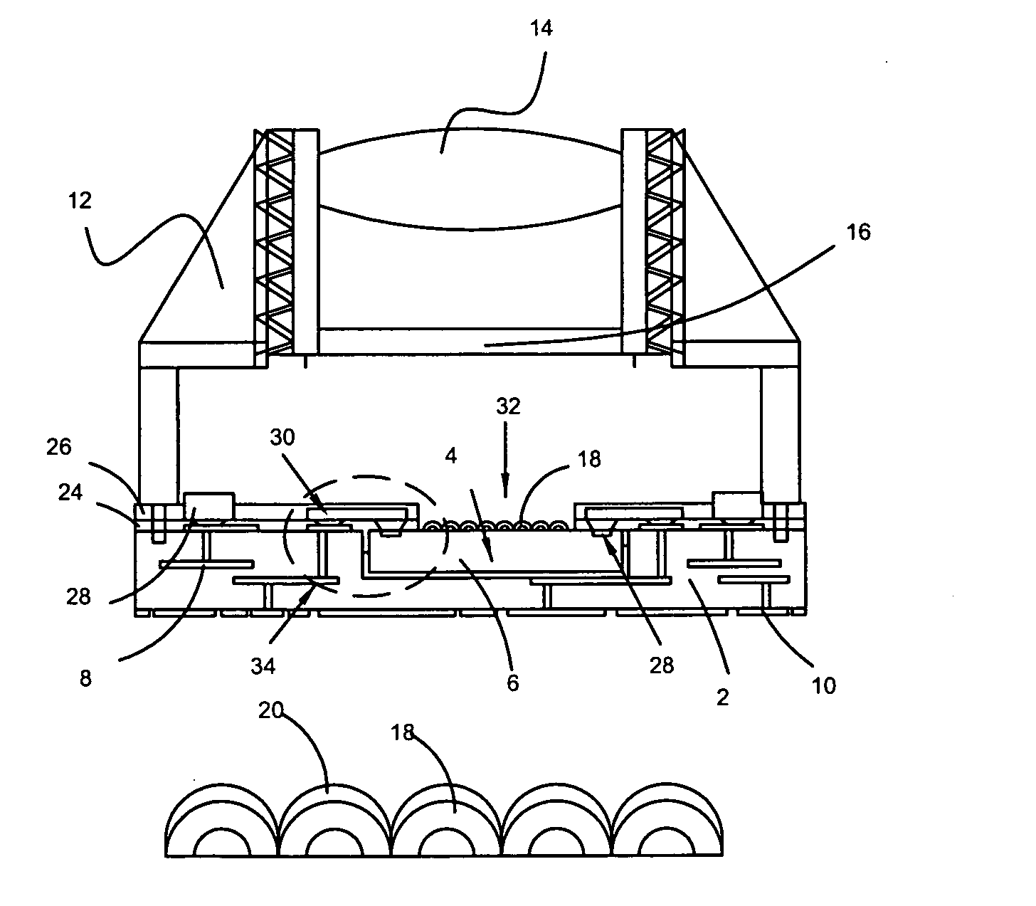
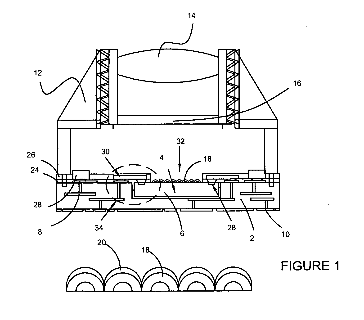
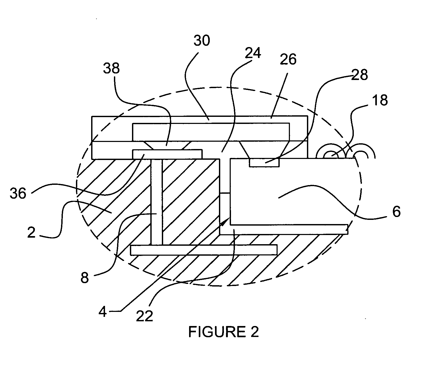
[0022]The present invention discloses a structure of an image sensor module utilizing a substrate having predetermined cavity formed into the substrate. A photosensitive material is coated over the die and the pre-formed substrate. Preferably, the material of the photosensitive material is formed of elastic material. The image sensor module comprising PCB mother board with cavity for Image Sensor chip and build up layers are employed. The module with super thin structure is less t...


PUM


Abstract

The present invention provides an image sensor module structure comprising a substrate with a die receiving cavity formed within an upper surface of the substrate and conductive traces within the substrate and a die having a micro lens disposed within the die receiving cavity. A dielectric layer is formed on the die and the substrate, a re-distribution conductive layer (RDL) is formed on the dielectric layer, wherein the RDL is coupled to the die and the conductive traces and the dielectric layer has an opening to expose the micro lens. A lens holder is attached on the substrate and the lens holder has a lens attached an upper portion of the lens holder. A filter is attached between the lens and the micro lens. The structure further comprises a passive device on the upper surface of the substrate within the lens holder.

Description

FIELD OF THE INVENTION[0001]This invention relates to a structure of image sensor, and more particularly to an image sensor module with die receiving cavity.DESCRIPTION OF THE PRIOR ART[0002]Digital video cameras are under development to facilitate as home appliances. Due to the quick development of the semiconductor technology, the application of the image sensor is widely used for digital still camera or movie camera. Consumers' demand has been directed to light weight, multi-function and high resolution. To meet such demand, technical levels of manufacturing camera have been improved. CCD or CMOS chip is popular device for these camera to capture image and die-bonded by means of a conductive adhesive. Typically, an electrode pad of the CCD or CMOS is wire-bonded by means of a metal wire. The wire bonding limits the size of the sensor module. The device is formed by traditional resin packaging method.[0003]A commonly used conventional image sensor device has an array of photodiode...

Claims


Application Information

Patent Timeline
IPC IPC(8): H01L27/00
CPCH01L27/14618H01L27/14625H01L27/14634H01L24/18H01L27/1469H04N5/2253H04N5/2257H01L27/14636H01L2924/14H01L2224/04105H01L2224/12105H01L2224/24195H01L2224/73267H01L2924/15153H01L24/82H01L2924/19105H01L24/24H04N23/57H04N23/54H01L2924/00H01L27/146
Inventor YANG, WEN-KUNCHANG, JUI-HSIENWANG, TUNG-CHUANLIN, CHIHWEIHSU, HSIEN-WEN
Owner ADVANCED CHIP ENG TECH
Why Eureka
Try Eureka