

LED chip package structure with a plurality of thick guiding pins and a method for manufacturing the same
- Summary
- Abstract
- Description
- Claims
- Application Information
AI Technical Summary
Benefits of technology
Problems solved by technology
Method used
Image

Examples
first embodiment
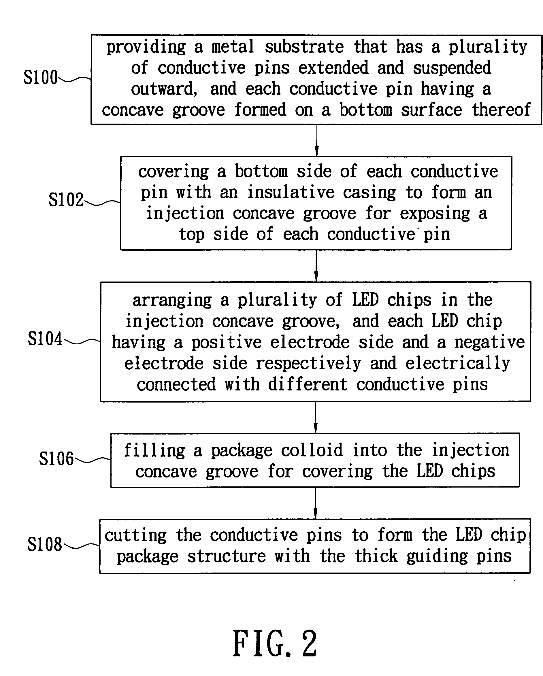
[0043]Referring to FIGS. 2 to 5, the present invention provides a method for manufacturing an LED chip package structure with a plurality of thick guiding pins.
[0044]The method comprises: firstly, referring to FIG. 3, providing a metal substrate 1 that has a plurality of conductive pins 11 extended and suspended outward, and each conductive pin 11 having a concave groove 111 formed on a bottom surface thereof (S100). The conductive pins 11 are separated from each other. Each concave groove 111 can be a half etching concave groove. The metal substrate 1 and the conductive pins 11 are formed via an etching method, a punching method, or any forming method. The metal substrate 1 has an electroplated protection layer 110 formed on a surface thereof. It means that each conductive pin 11 has an electroplated protection layer 110 formed on a surface thereof. In addition, each conductive pin 11 has a thickness between 0.4 mm and 3 mm. Of course, the thickness of each conductive pin 11 should...
second embodiment
[0053]Referring to FIGS. 15 and 16, the present invention provides a method for manufacturing an LED chip package structure with a plurality of thick guiding pins. The method comprises: firstly, referring to FIG. 16, providing a metal substrate 1′ that has a plurality of conductive pins 11′ extended outward to fix two lateral sides of each conductive pin 11′, and each conductive pin 11′ having a concave groove 111′ formed on a bottom surface thereof (S200). Each concave groove 111′ can be a half etching concave groove. After the step of S200, the method further comprises: covering a bottom side of each conductive pin 11′ with an insulative casing 2′ to form an injection concave groove 20′ for exposing a top side of each conductive pin 11′ (S202). The insulative casing 2′ is filled into a plurality of non-conductive areas 21′ between each two conductive pins 11′.
[0054]Furthermore, the next steps of the second embodiment are same as the steps of S104 to S108 in the first embodiment. T...
third embodiment
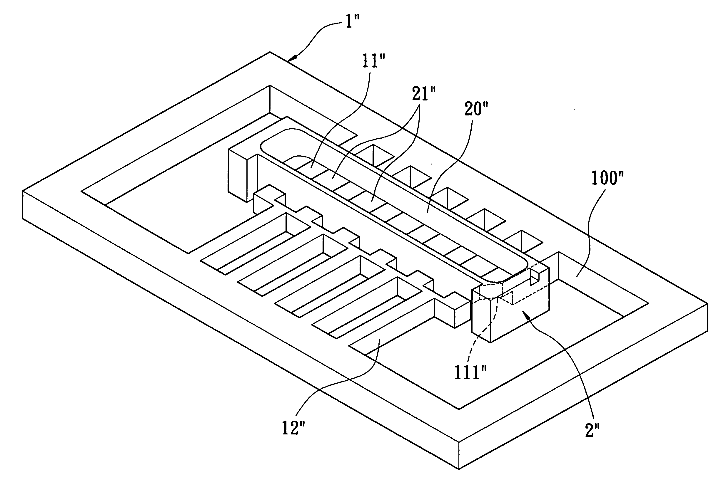
[0055]Referring to FIGS. 17 and 18, the present invention provides a method for manufacturing an LED chip package structure with a plurality of thick guiding pins. The method comprises: firstly, referring to FIG. 18, providing a metal substrate 1″ that has a plurality of conductive pins 11″ extended and suspended outward and a plurality of strengthening ribs 12″ joint between each two conductive pins 11″, and each conductive pin 11″ has a concave groove 111″ formed on a bottom surface thereof (S300). Each concave groove 111″ can be a half etching concave groove. After the step of S300, the method further comprises: covering a bottom side of each conductive pin 11″ with an insulative casing 2″ to form an injection concave groove 20″ for exposing a top side of each conductive pin 11″ (S302). The insulative casing 2″ is filled into a plurality of non-conductive areas 21″ between each two conductive pins 11″.
[0056]Furthermore, the next steps of the second embodiment are same as the step...
PUM
 Abstract
Description
Claims
Application Information