Systems and methods for kickback reduction in an ADC

a technology of system and method, applied in the field of analog to digital conversion, can solve the problems of low oversampling ratio, general inability to adequately operate, and circuits with a tendency to be very noisy, so as to reduce or eliminate noise, reduce or eliminate the effect of kickback nois

Active Publication Date: 2008-07-31
TEXAS INSTR INC
View PDF11 Cites 0 Cited by
  • Summary
  • Abstract
  • Description
  • Claims
  • Application Information

AI Technical Summary

Benefits of technology

[0009]In some instances of the aforementioned embodiments, the kickback filter is a buffer, while in other instances of the aforementioned embodiments the kickback filter is a band pass filter. Such a kickback filter is operable to reduce or eliminate noise evident at the input of the second summation element from kicking back onto the input signal. In some instances of the aforementioned embodiments, another integrator is electrically coupled between the first integrator and the second summation element. In such cases, the second integrator is electrically coupled to the summation element. In some instances of the aforementioned embodiments, the integrators are implemented with a switch network on either side of a sampling capacitor.
[0010]Other embodiments of the present invention provide kickback limited Delta-Sigma Modulators. Such kickback limited Delta-Sigma Modulators include an integrator, a first summation element and a second summation element, and an analog to digital converter. An output of the first summation element is electrically coupled to the integrator; an output of the analog to digital converter is electrically coupled to the first summation element; and an output of the second summation element is electrically coupled to the analog to digital converter. An input signal is applied to the first summation element directly, and to the second summation element via a kickback filter. The kickback filter is operable to reduce or eliminate kickback noise from the node electrically coupled to the second summation element to the input signal.
[0013]Yet other embodiments of the present invention provide methods for reducing kickback in an analog to digital converter. Such methods include providing an integrator, an analog to digital converter, a first summation element and a second summation element. The methods further include electrically coupling an output of the first summation element to the integrator; electrically coupling an output of the analog to digital converter to the first summation element; electrically coupling an output of the second summation element to the analog to digital converter; applying an input signal to the first summation element; and applying the input signal to the second summation element via a kickback filter. In such cases, the kickback filter is operable to limit noise coupling between the second summation element and the input signal.

Problems solved by technology

In contrast, analog to digital conversion system 100 does not work well at low oversampling ratios (i.e., oversampling ratios less than eight to sixteen) due primarily to non-linearities caused by variations in manufacturing processes and circuit imperfections.
In some cases, analog to digital conversion system 100 has been implemented with high quality analog components to address some of the causes of the aforementioned non-linearities, however, even with the use of such high quality components analog to digital conversion system 100 is generally not capable of adequate operation a low oversampling rates (i.e., eight to sixteen or less).
This is because the circuit has a tendency to be very noisy at or near the band of interest.
The level of noise seems to be less when the circuit is used at relatively high oversampling rates (i.e., eight to sixteen or greater), but renders the circuit unreliable at lower oversampling rates.

Method used


Image

  • Systems and methods for kickback reduction in an ADC
  • Systems and methods for kickback reduction in an ADC
  • Systems and methods for kickback reduction in an ADC

Examples


Embodiment Construction

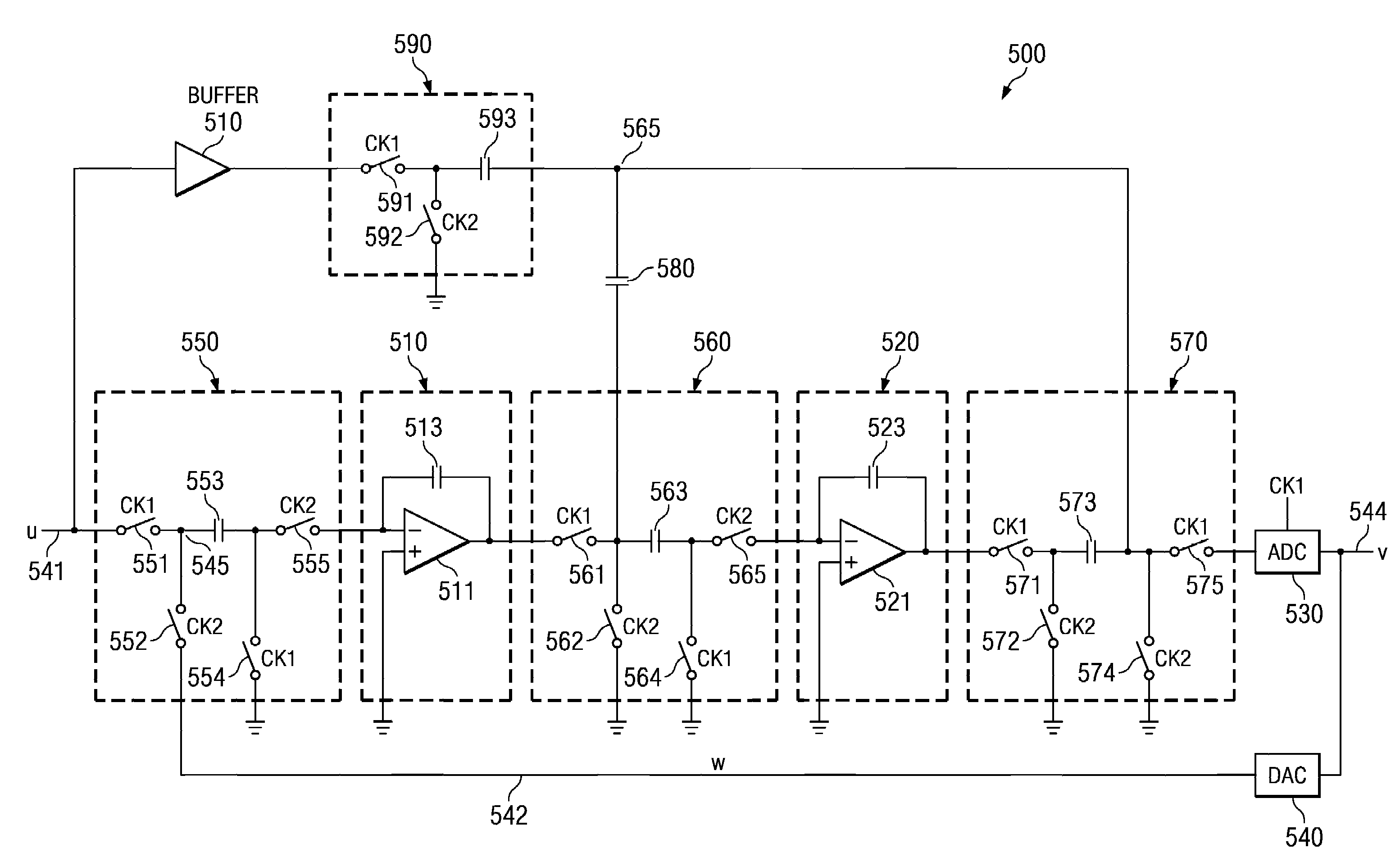
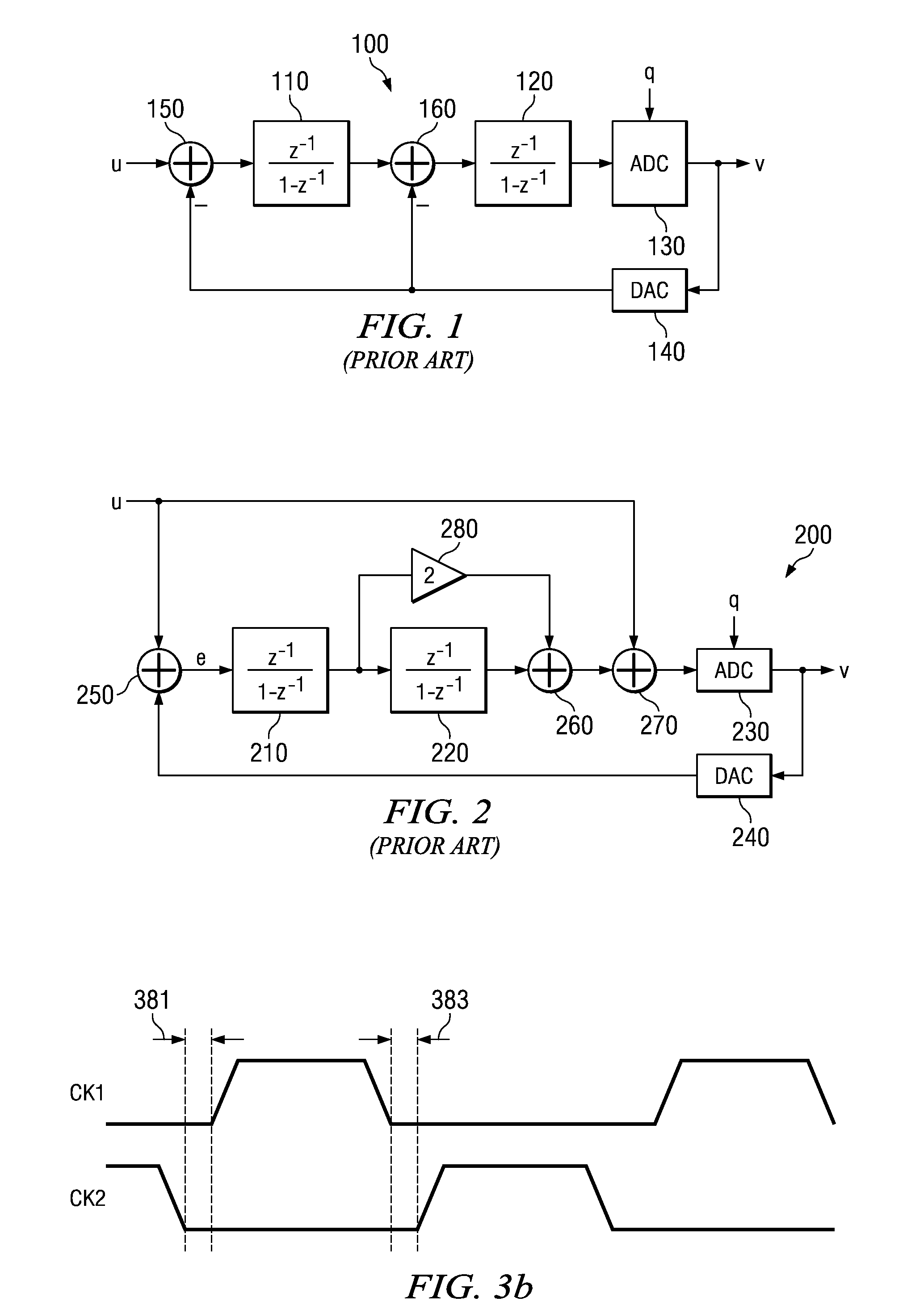
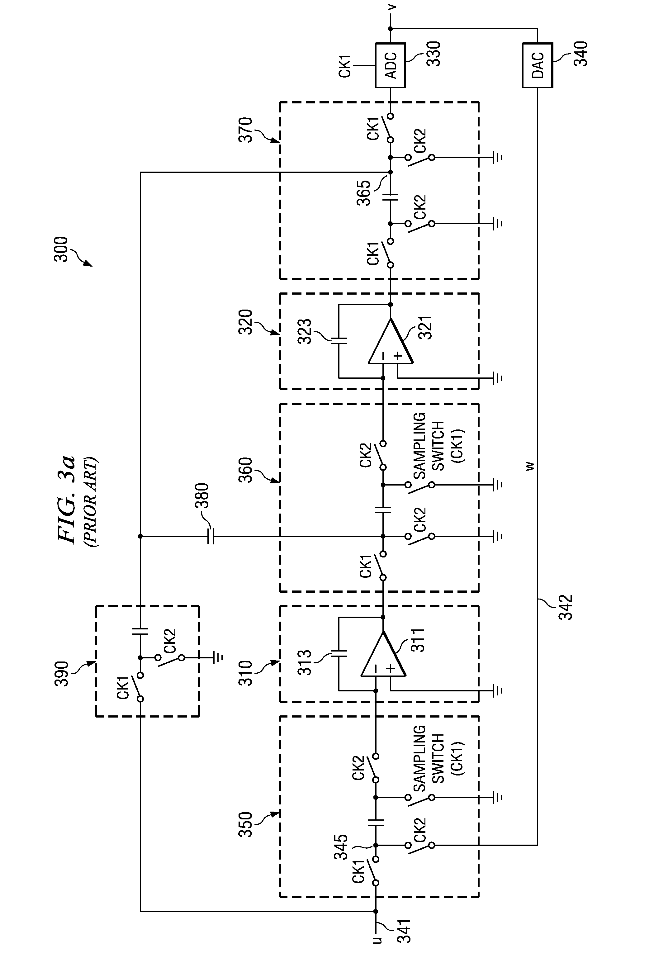
[0024]The present invention is related to analog to digital conversion, and more particularly to systems and methods for reducing kickback in relation to analog to digital conversion.

[0025]Various systems and methods for analog to digital conversion are disclosed. For example, some embodiments of the present invention provide analog to digital conversion systems based on Delta-Sigma modulation. Some such analog to digital conversion systems include a Delta-Sigma modulator with a feed forward path that electrically couples an analog voltage input to a summation element directly preceding an analog to digital converter that provides a digital representation of the input. The analog input is electrically coupled to the summation element via a kickback filter that eliminates or reduces the amount of noise at or around the summation element that can be introduced back onto the input signal. This allows the analog to digital conversion system to operate at higher frequencies without undue...


PUM


Abstract

Various systems and methods for analog to digital conversion are disclosed. For example, some embodiments of the present invention provide analog to digital conversion systems. The analog to digital conversion systems include a first integrator and a second integrator, and a first summation element and a second summation element. An output of the first summation element is electrically coupled to the first integrator, and an output of the first integrator is electrically coupled to the second integrator. An output of the second integrator is electrically coupled to the second summation element. The analog to digital conversion systems further include an analog to digital converter that is electrically coupled to the first summation element via a digital to analog converter. An input to the analog to digital conversion system is electrically coupled to the first summation element, and the input is electrically coupled to the second summation element via a kickback filter.

Description

BACKGROUND OF THE INVENTION[0001]The present invention is related to analog to digital conversion, and more particularly to systems and methods for reducing kickback in relation to analog to digital conversion.[0002]Turning to FIG. 1, an analog to digital conversion system 100 including a Delta-Sigma Modulator is shown. Analog to digital conversion system 100 includes two integrators 110, 120, two summation elements 150, 160, a digital to analog converter 140, and an analog to digital converter 130. An input signal (u) and a feedback signal from digital to analog converter 140 are aggregated by summation element 150. The aggregate from summation element 150 is applied to integrator 110. The output of integrator 110 is aggregated with the feedback signal from digital to analog converter 140 using summation element 160. The aggregate from summation element 160 is applied to integrator 120, and the output of integrator 120 is applied to analog to digital converter 130. The output (v) o...

Claims


Application Information

Patent Timeline
Patent Type & Authority Applications(United States)
IPC IPC(8): H03M3/00H03M1/12
CPCH03M3/376H03M3/45H03M3/452
Inventor KOE, WERN M.PARK, YONG-IN
Owner TEXAS INSTR INC
Why Eureka
Try Eureka