Liquid crystal display device and method of manufacturing the same

a liquid crystal display and display device technology, applied in non-linear optics, instruments, optics, etc., can solve the problems of small viewing angle, large retention volume, and decrease in transmission and the like, and achieve the effect of increasing the number of manufacturing steps

Active Publication Date: 2008-07-31
JAPAN DISPLAY INC
View PDF6 Cites 47 Cited by
  • Summary
  • Abstract
  • Description
  • Claims
  • Application Information

AI Technical Summary

Benefits of technology

[0011]An advantage of some aspects of the invention is to provide an FFS mode liquid crystal display device in which a plurality of contact holes can be formed on a single step when a pixel electrode and a common electrode are disposed on a planarization film, and which has a high aperture ration and a high display image quality.

Problems solved by technology

However, a twisted nematic (TN) mode generally used in such liquid crystal display devices of a vertical electric field system has a problem in that the viewing angle is small.
However, IPS mode liquid crystal display devices have the problem that the liquid crystal molecules above the pixel electrode are not sufficiently driven due to the pair of electrodes being provided in a singe layer for applying an electric field to the liquid crystals, resulting in a decrease in transmission and the like.
In addition, FFS mode liquid crystal display devices have a larger area in which the pixel electrode and the common electrode overlap in planar view compared to IPS mode liquid crystal display devices, further resulting in a larger retention volume.
However, since a step is formed on the surface of the pixel electrode which overlaps with a switching element or a common line in a related-art FFS mode liquid crystal display device, liquid crystal molecules are misaligned in the step portion.
Thus, there is a problem in that separate steps are necessary to form the contact holes.

Method used


Image

  • Liquid crystal display device and method of manufacturing the same
  • Liquid crystal display device and method of manufacturing the same
  • Liquid crystal display device and method of manufacturing the same

Examples


first embodiment

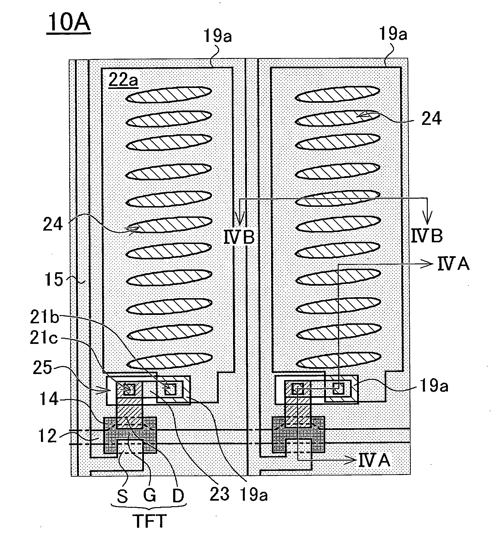
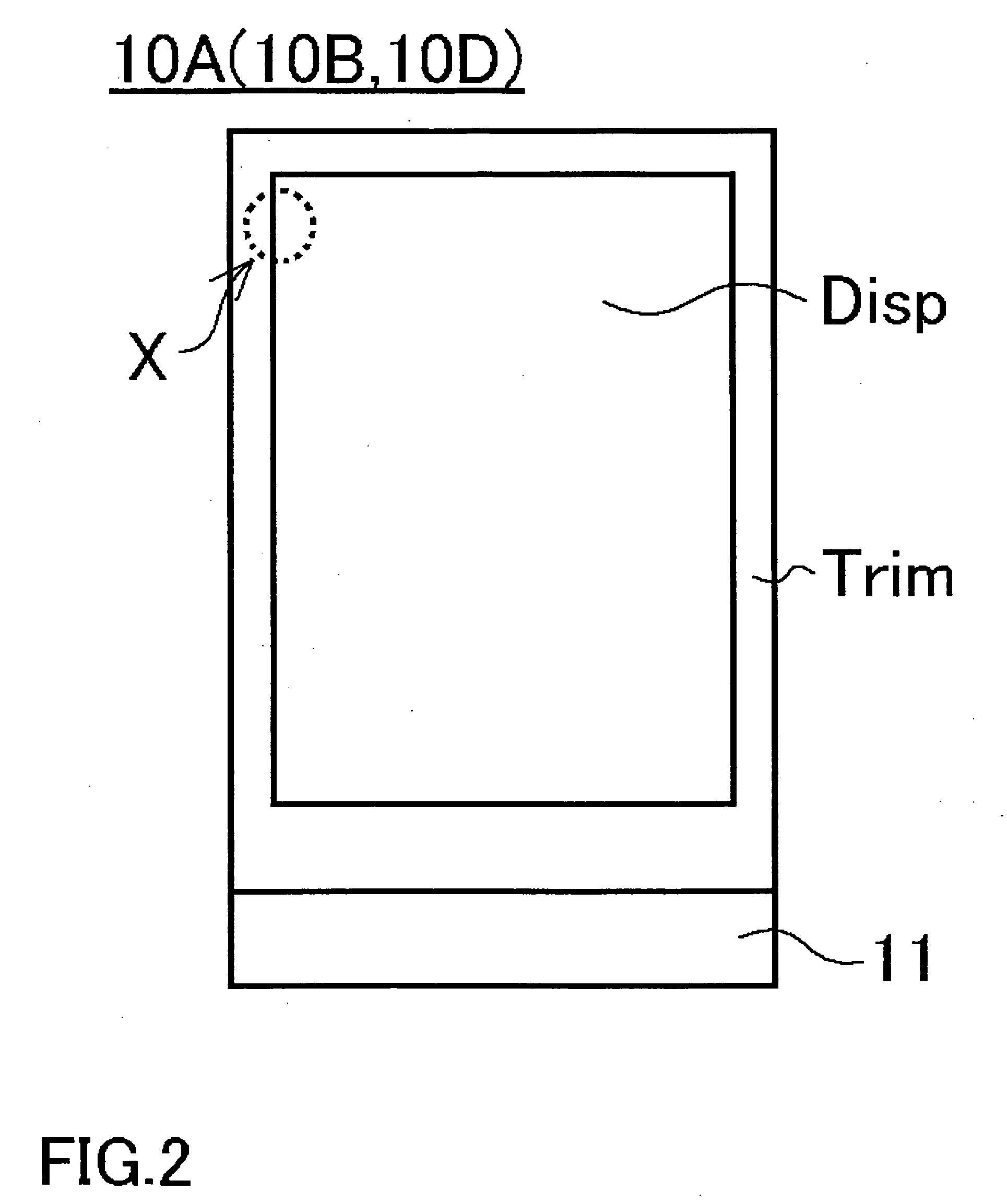
[0053]As an FFS mode liquid crystal display device according to a first embodiment, an FFS mode liquid crystal display device which includes a planarization film and in which an upper electrode as a common electrode is connected with a common line is described in the order of the manufacturing steps using FIGS. 1 to 5. FIG. 1 is a schematic plan view showing two pixels of an array substrate of a liquid crystal display device 10A according to the first embodiment. FIG. 2 is a view showing a connection position X of the common line and the common electrode of the liquid crystal display device according to the first embodiment. FIG. 3 is an enlarged plan view of the array substrate at an X portion of the liquid crystal display device 10A according to the first embodiment. FIG. 4A is a schematic sectional view along the line IVA-IVA of FIG. 1, FIG. 4B is a schematic sectional view along the line IVB-IVB of FIG. 1, and FIG. 4C is a schematic sectional view along the line IVC-IVC of FIG. ...

second embodiment

[0069]Next, an example of an FFS mode liquid crystal display device according to a second embodiment, which includes a planarization film and in which a lower electrode as a common electrode is connected with a common line, is described in the order of the manufacturing steps using FIGS. 6 to 9. FIG. 6 is a schematic plan view showing two pixels of an array substrate of the liquid crystal display device according to the second embodiment. FIG. 7 is an enlarged plan view of the array substrate at a connection position between the common line and the common electrode of the liquid crystal display device according to the second embodiment. FIG. 8A is a schematic sectional view along the line VIIIA-VIIIA of FIG. 6, and FIG. 8B is a schematic sectional view along the line VIIIB-VIIIB of FIG. 7. FIG. 9 is an enlarged plan view of the array substrate at a connection position for connecting with the common electrode in a modified example of a liquid crystal display device 10B according to t...


PUM

PropertyMeasurementUnit
transparentaaaaaaaaaa
conductiveaaaaaaaaaa
vertical electric fieldaaaaaaaaaa

Abstract

A method of manufacturing a liquid crystal display device 10A according to an embodiment of the present invention includes: forming a pixel electrode 19a for each sub-pixel on the surface of a planarization film 18, forming an insulator 20 over the whole surface, simultaneously forming first to third contact holes 21a to 21c so that a drain electrode D, a connection portion 161 of a common line, and the pixel electrode 19a are exposed from the surface of the insulator 20, forming a film of a transparent conductive material over the whole surface, forming a common electrode 22a including a plurality of slits for each sub-pixel, and connecting the common electrode 22 and the connection portion 161 via the first contact hole 21a and connecting the pixel electrode 19a and the drain electrode D via an interface-structured conductive path 23 formed via the second contact hole 21b, the surface of the insulator 20, and the third contact hole 21c. Accordingly, the invention provides an FFS mode liquid crystal display device and a method of manufacturing the same in which the plurality of contact holes can be formed simultaneously in a single step and the pixel electrode and the common electrode are disposed on the planarization film.

Description

BACKGROUND[0001]1. Technical Field[0002]The present invention relates to an FFS mode liquid crystal display device which can be manufactured without increasing the number of manufacturing steps, and can achieve a high aperture ratio and high display image quality with a pixel electrode and a common electrode disposed on a planarization film, and a method of manufacturing the same.[0003]2. Related Art[0004]Liquid crystal display devices of a vertical electric field system including a pair of transparent substrates having an electrode and the like formed on the surface, and a liquid crystal layer held between the pair of substrates, in which various pieces of information are displayed by applying voltage to the electrodes on the substrates to realign liquid crystals, have been popularly used. However, a twisted nematic (TN) mode generally used in such liquid crystal display devices of a vertical electric field system has a problem in that the viewing angle is small. Therefore, various...

Claims


Application Information

Patent Timeline
Patent Type & Authority Applications(United States)
IPC IPC(8): G02F1/13G02F1/1343
CPCG02F1/134309G02F1/136227G02F2201/40G02F2001/134372G02F2001/134381G02F2001/133357G02F1/133357G02F1/134372G02F1/134381G02F1/133G02F1/136
Inventor HORIGUCHI, MASAHIROKANEKO, HIDEKI
Owner JAPAN DISPLAY INC
Why Eureka
Try Eureka