Electronics Package And Manufacturing Method Thereof

Inactive Publication Date: 2008-08-07
NOKIA CORP
View PDF5 Cites 23 Cited by
  • Summary
  • Abstract
  • Description
  • Claims
  • Application Information

AI Technical Summary

Benefits of technology

[0004]The invention enables electronics miniaturization, i.e. less weight, less volume, smaller size, as well as having more functions, reduced manufac

Problems solved by technology

Electronics packages are therefore big in relation to their active area, as well as having a large volume and a

Method used


Image

  • Electronics Package And Manufacturing Method Thereof
  • Electronics Package And Manufacturing Method Thereof
  • Electronics Package And Manufacturing Method Thereof

Examples


Embodiment Construction

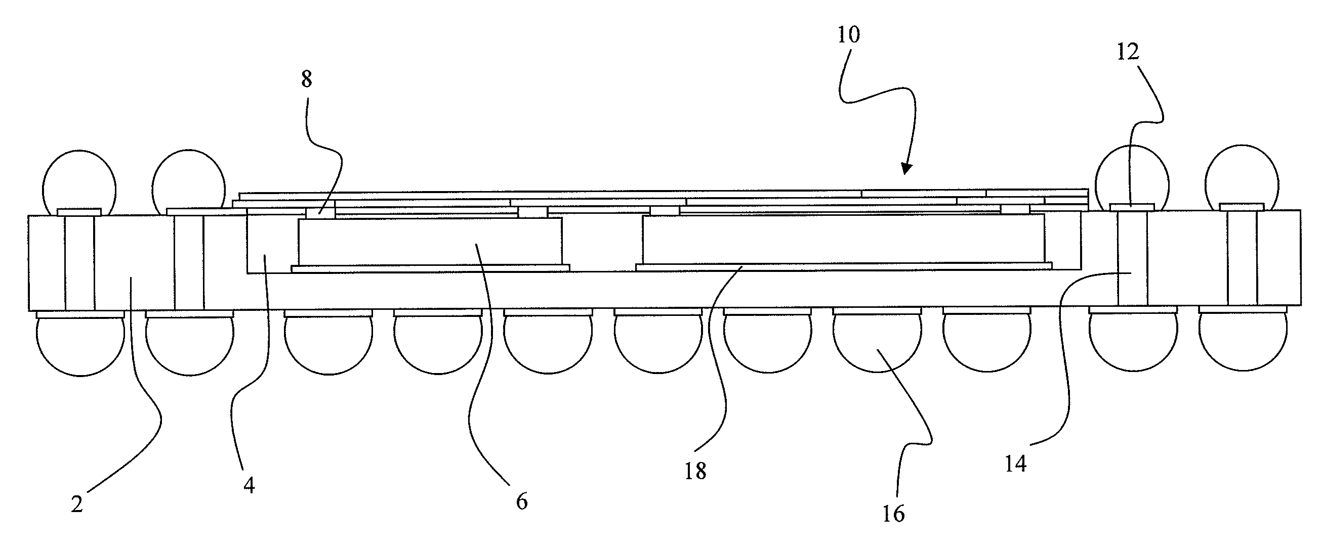
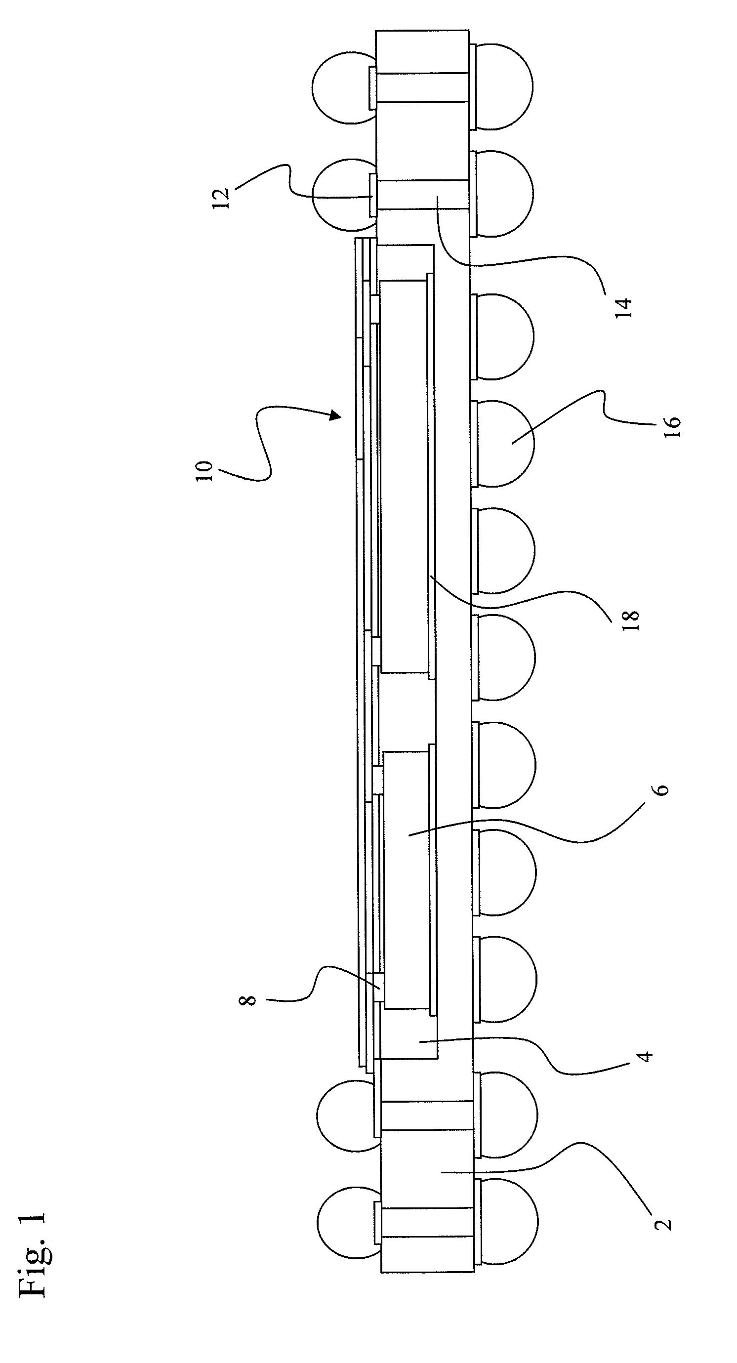
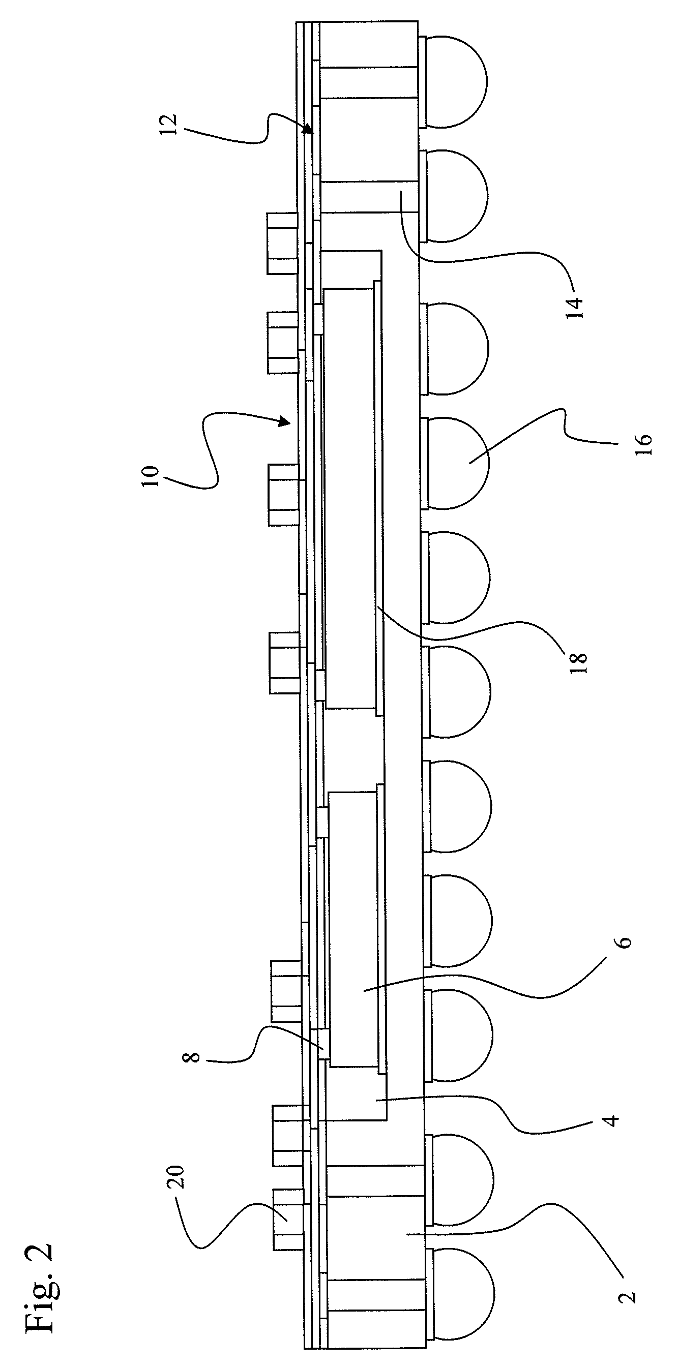
[0061]The invention enables a miniaturization of electronics packages using bare die components and other components fitting inside a module, and by arranging several components in a single module. A stacked electronics package according to the invention consists of functional blocks or modules that are stacked on top of each other. Different product variations can be made using personalized blocks in a stacked package.

[0062]A module according to one embodiment of the invention consists of a carrier substrate having a recess in which components are attached. The recess is filled up with molding compound so that the connection pads of the components are exposed facing upwards. The wirings of a module that are connected to the connection pads are formed using inkjet printed conductive and dielectric materials. The module can be used as single module or as a stackable functional block to be stacked together with other functional blocks.

[0063]It is to be noted that the recess in the car...


PUM

PropertyMeasurementUnit
Structureaaaaaaaaaa
Electrical conductoraaaaaaaaaa
Areaaaaaaaaaaa

Abstract

A method for manufacturing an electronics package is provided that comprises forming at least one module block by providing a carrier substrate having a recess, placing at least one electronic component die in said recess, filling said recess with a molding material, and depositing a circuit layer connected with said at least one component die. It further provides an electronics package, comprising a carrier substrate having a recess, at least one electronic component die placed in said recess, a molding material filling said recess, and a circuit layer connected with said at least one component die.

Description

[0001]The invention relates in general to printed electronics, microelectronics packaging, integration and miniaturization of electronics. It is particularly concerned with an electronics package and the manufacturing method thereof.PRIOR ART[0002]Usually electronics components are packaged, but the active die area inside a package can be as low as 10% of the overall package size. Electronics packages are therefore big in relation to their active area, as well as having a large volume and also a high weight.[0003]Prior art electronics modules use substrates that are made using conventional printed wiring board (PWB) techniques, or using ceramic substrates. Components are attached using surface-mount technology (SMT), flip chip, tape automated bonding (TAB) or wire bonding. These processes are material consuming and their related time to market is considerably long.SUMMARY OF THE INVENTION[0004]The invention enables electronics miniaturization, i.e. less weight, less volume, smaller ...

Claims


Application Information

Patent Timeline
IPC IPC(8): H05K1/18H05K3/30
CPCH01L23/13Y10T29/49146H01L23/49827H01L23/50H01L23/5389H01L23/552H01L24/24H01L24/82H01L25/105H01L2223/6677H01L2224/24011H01L2224/24137H01L2224/24227H01L2224/76155H01L2924/01082H01L2924/15153H01L2924/15165H01L2924/15311H01L2924/15331H01L2924/19104H01L2924/19106H01L2924/3025H05K1/023H05K1/144H05K1/185H05K3/125H05K3/4664H05K2203/013H01L23/49816Y10T29/49126H01L2225/1035H01L2224/92244H01L2924/01033H01L2924/014H01L24/83H01L25/16H01L2225/1058H01L2224/73267H01L2224/83H01L2224/82102H01L2224/32225H01L2924/181H01L2924/00
Inventor MIETTINEN, JANIMANSIKKAMAKI, PAULIINAMOLKKARI, PETRIMANTYSALO, MATTIVALTANEN, JANI
Owner NOKIA CORP
Why Eureka
Try Eureka