Glass dam structures for imaging devices chip scale package

a technology of microelectronic imager and scale package, which is applied in the direction of semiconductor devices, electrical equipment, semiconductor/solid-state device details, etc., can solve the problems of increasing the vertical thickness of conventional packaged microelectronic imagers, limiting the design and marketability of compact picture cell phones or pdas, and increasing manufacturing costs and process complexity

Inactive Publication Date: 2008-08-14
VISERA TECH CO LTD
View PDF4 Cites 20 Cited by
  • Summary
  • Abstract
  • Description
  • Claims
  • Application Information

AI Technical Summary

Benefits of technology

[0010]A detailed description is given in the following embodiments with reference to the accompanying drawings. These and other problems are generally s...

Problems solved by technology

Conventional packaged optoelectronic microstructure elements can present increased manufacturing costs and process complexity.
Accordingly, the increased ve...

Method used


Image

  • Glass dam structures for imaging devices chip scale package
  • Glass dam structures for imaging devices chip scale package
  • Glass dam structures for imaging devices chip scale package

Examples


Embodiment Construction

[0018]The following description is of the best-contemplated mode of carrying out the invention. This description is made for the purpose of illustrating the general principles of the invention and should not be taken in a limiting sense.

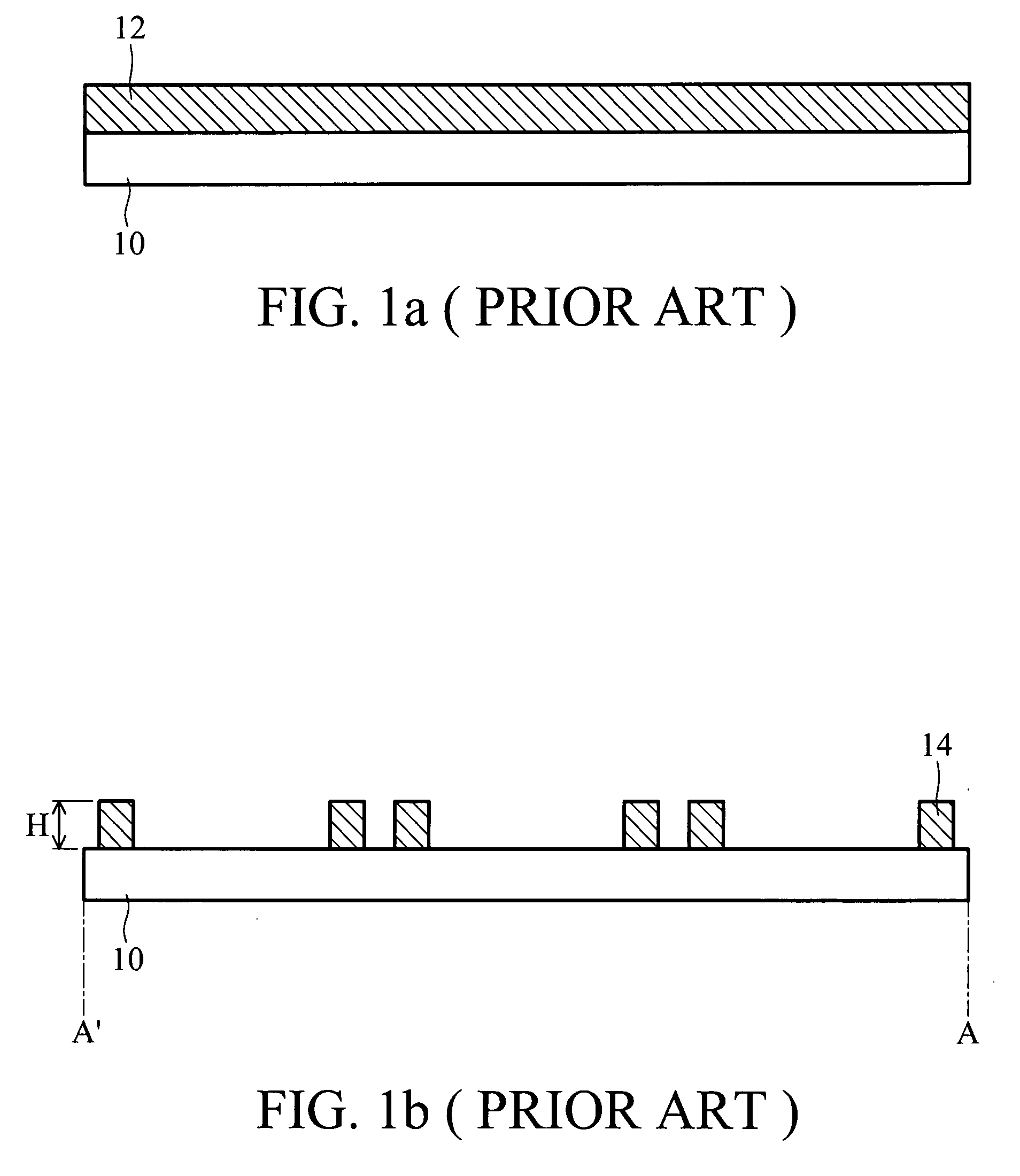
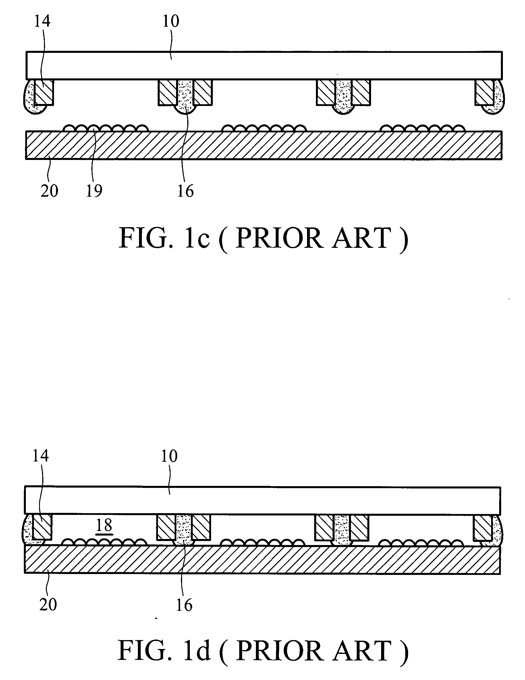
[0019]FIGS. 3a-3m are cross sections illustrating an exemplary embodiment of a method for fabricating a CMOS image sensor chip scale package of the invention.

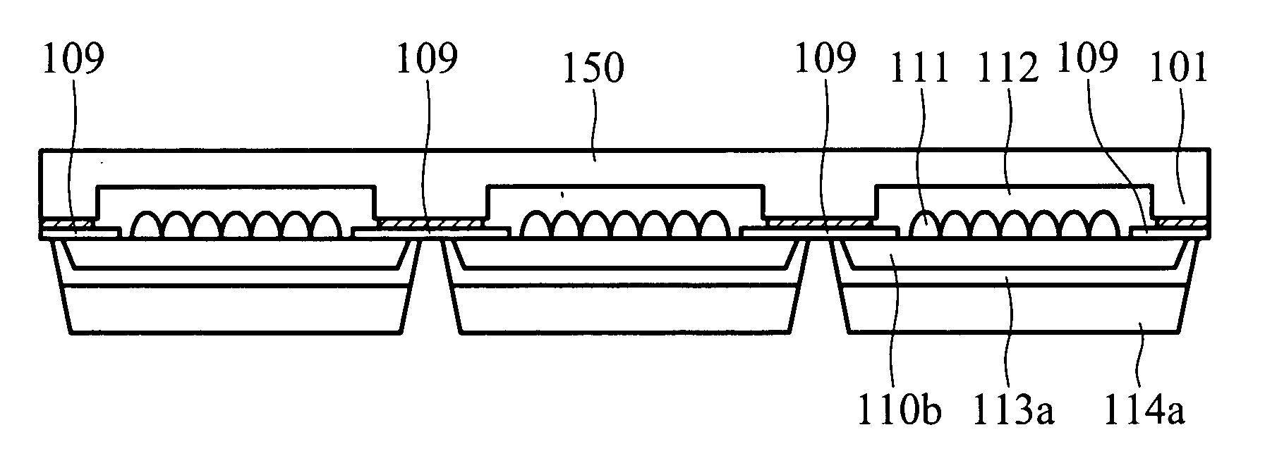
[0020]Referring to FIG. 3a, a glass substrate 100 is provided. Next, referring to FIG. 3b, the glass substrate 100 is partially removed by bulk micromachining to form a glass encapsulant 150 having openings 102 and dam structures 101 surrounding the opening 102. FIG. 4 is a schematic diagram of the glass encapsulant 150, and FIG. 3b is a sectional diagram of FIG. 4 along lines B-B′. Referring to FIG. 4, the profile of the sidewall 104 of the dam structure 101 is straight, and the opening 102 is square. In some embodiments of the invention, the profile of the sidewall 104 of the dam structure 101...


PUM


Abstract

Glass dam structures for imaging device chip scale package. An optoelectronic device chip scale package comprises a substrate configured as a support structure for the chip scale package. A semiconductor die with die circuitry is attached to the substrate. A glass encapsulant is disposed on the substrate encapsulating the semiconductor die, wherein the glass encapsulant has a dam structure around an opening. A seal layer is disposed between the substrate and the dam structure bonding the two together.

Description

BACKGROUND OF THE INVENTION[0001]1. Field of the Invention[0002]The invention relates to an optoelectronic device chip scale packages, and more particularly to a CMOS image sensor chip scale package.[0003]2. Description of the Related Art[0004]Microelectronic imagers are used in digital cameras, wireless devices with picture capabilities, and many other applications. Cell phones and Personal Digital Assistants (PDAs), for example, incorporate microelectronic imagers for capturing and sending digital images. The use of microelectronic imagers in electronic devices has been steadily increasing as imagers become smaller and produce higher quality images with increased pixel counts.[0005]Microelectronic imagers include image sensors that use Charged Coupled Device (CCD) systems, Complementary Metal-Oxide Semiconductor (CMOS) systems, or other systems. CCD image sensors are widely used in digital cameras and other applications. CMOS image sensors are also becoming very popular due to low...

Claims


Application Information

Patent Timeline
IPC IPC(8): H01L23/02
CPCH01L27/14683H01L27/14618H01L2224/0554H01L2224/05548H01L2224/05573H01L2224/13H01L2924/00014H01L2924/16235H01L2224/05599H01L2224/0555H01L2224/0556
Inventor LEE, HSIAO-WENWENG, JUI-PING
Owner VISERA TECH CO LTD
Why Eureka
Try Eureka