
Mos transistors having recessed channel regions and methods of fabricating the same

a channel region and transistor technology, applied in the field ofmos transistors, can solve the problem that the current drivability of the recessed channel transistor is inferior to that of the planar transistor, and achieve the effect of high carrier mobility and recessed channel regions

Inactive Publication Date: 2008-08-28
SAMSUNG ELECTRONICS CO LTD
View PDF5 Cites 13 Cited by
  • Summary
  • Abstract
  • Description
  • Claims
  • Application Information

AI Technical Summary

Benefits of technology

[0009]An embodiment of the present invention provides a MOS transistor having high carrier mobility and recessed channel regions. In embodiments of the invention, a recessed channel region is formed using a gate trench structure disposed in the active region between the source and drain regions. A semiconductor region is formed on the gate trench structure using a different material from the active region to provide high carrier mobility.
[0010]Another embodiment of the present invention provides a method of fabricating a MOS transistor having high carrier mobility and recessed channel regions.

Problems solved by technology

That is, the recess-channel transistor is inferior in current drivability with respect to the planar transistor.

Method used


Image

  • Mos transistors having recessed channel regions and methods of fabricating the same
  • Mos transistors having recessed channel regions and methods of fabricating the same
  • Mos transistors having recessed channel regions and methods of fabricating the same

Examples


Embodiment Construction

[0020]The present invention will now be described more fully hereinafter with reference to the accompanying drawings, in which exemplary embodiments of the invention are shown. This invention may, however, be embodied in different forms and should not be construed as limited to the embodiments set forth herein. Rather, these embodiments are provided so that this disclosure is thorough and complete and fully conveys the scope of the invention to those skilled in the art. In the drawings, the thicknesses of layers and regions are exaggerated for clarity. The same reference numerals are used to denote the same elements.

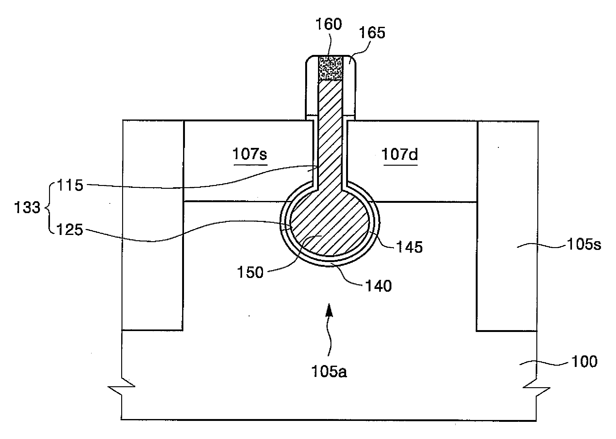
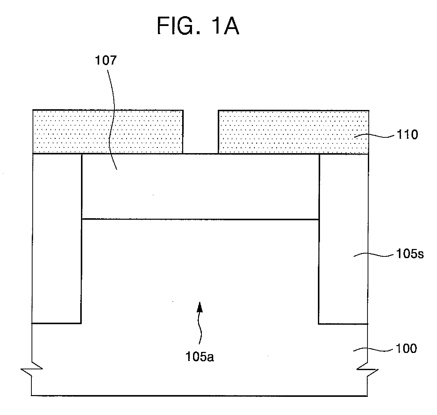
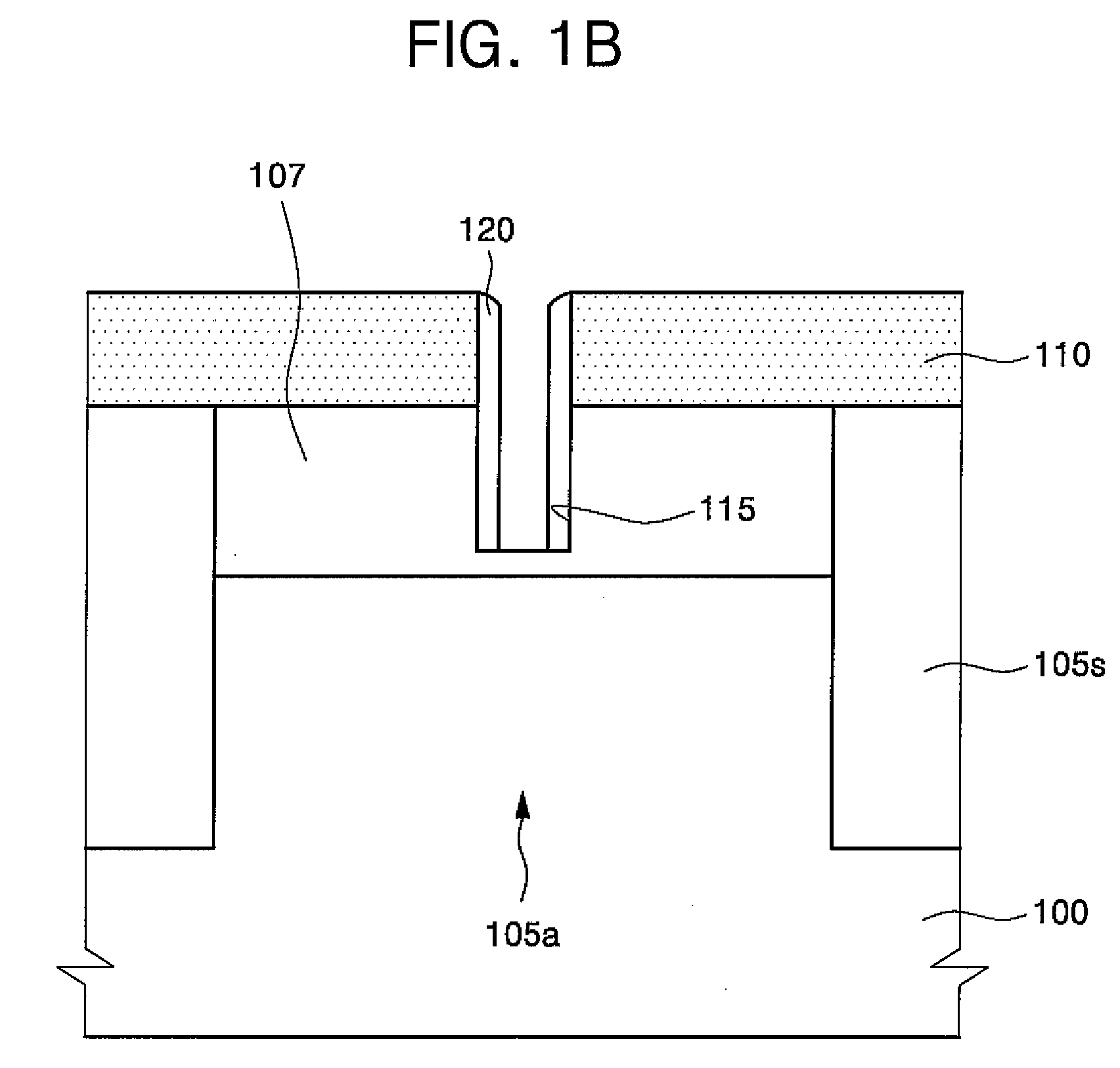
[0021]FIGS. 1A through 1F are cross-sectional views of a MOS transistor according to an exemplary embodiment of the present invention. First, a MOS transistor according to an exemplary embodiment of the present invention will be described with reference to FIG. 1F.

[0022]Referring to FIG. 1F, an isolation layer 105s may be disposed in a semiconductor substrate 100 to defi...


PUM


Abstract

A MOS transistor having a recessed channel region is provided. A MOS transistor includes a source region and a drain region disposed in an active region of a semiconductor substrate and spaced apart from each other. A gate trench structure is disposed in the active region between the source and drain regions. A gate electrode is disposed in the gate trench structure. A gate dielectric layer is interposed between the gate trench structure and the gate electrode. A semiconductor region is disposed between the gate trench structure and the gate dielectric layer. The semiconductor region is formed of a different material from the active region. A method of fabricating the MOS transistor having a recessed channel region is also provided.

Description

CROSS-REFERENCE TO RELATED APPLICATION[0001]This application claims the benefit of Korean Patent Application No. 10-2007-0018443, filed on Feb. 23, 2007, the contents of which are hereby incorporated herein by reference in their entirety.BACKGROUND OF THE INVENTION[0002]1. Field of the Invention[0003]The present invention relates to a MOS transistor and a method of fabricating the same and, more particularly, to a MOS transistor having a recessed channel region and a method of fabricating the same.[0004]2. Description of Related Art[0005]Semiconductor devices have widely employed discrete devices, such as field effect transistors (FETs), as switching devices. Generally, the operating speed of a transistor depends on an activation current supplied to a channel region formed between a source region and a drain region. Conventionally, a planar transistor may be prepared by forming a gate electrode and source and drain regions in a device forming region of a substrate, i.e., an active r...

Claims


Application Information

Patent Timeline
Patent Type & Authority Applications(United States)
IPC IPC(8): H01L29/778H01L21/336
CPCH01L29/1054H01L29/66621H01L29/4236H01L29/1037
Inventor CHOI, JAY-BOK
Owner SAMSUNG ELECTRONICS CO LTD
Learn More