Stress buffer layer for packaging process

Inactive Publication Date: 2008-08-28
TAIWAN SEMICON MFG CO LTD
View PDF9 Cites 31 Cited by
  • Summary
  • Abstract
  • Description
  • Claims
  • Application Information

AI Technical Summary

Benefits of technology

[0008]In accordance with another aspect of the present invention, a semiconductor package structure includes a package substrate having a plurality of bumps attached thereon; a first die having a first surface and a second surface opposite the first surface, wherein the second surface of the first die is bonded to the package substrate through the plurali

Problems solved by technology

The conventional packaging processes, however, suffer drawbacks.
High stress is generated, which is partially induced by a high mismatch of the coefficients of thermal expansion (CTE) between silicon semiconductor dies and package substrates.
The stress causes several major reliability concerns.
First, the stress may incur delamination at the interfaces between the dies and the epoxy molding compounds, and between the epoxy molding compounds and the package substrat

Method used


Image

  • Stress buffer layer for packaging process
  • Stress buffer layer for packaging process
  • Stress buffer layer for packaging process

Examples


second embodiment

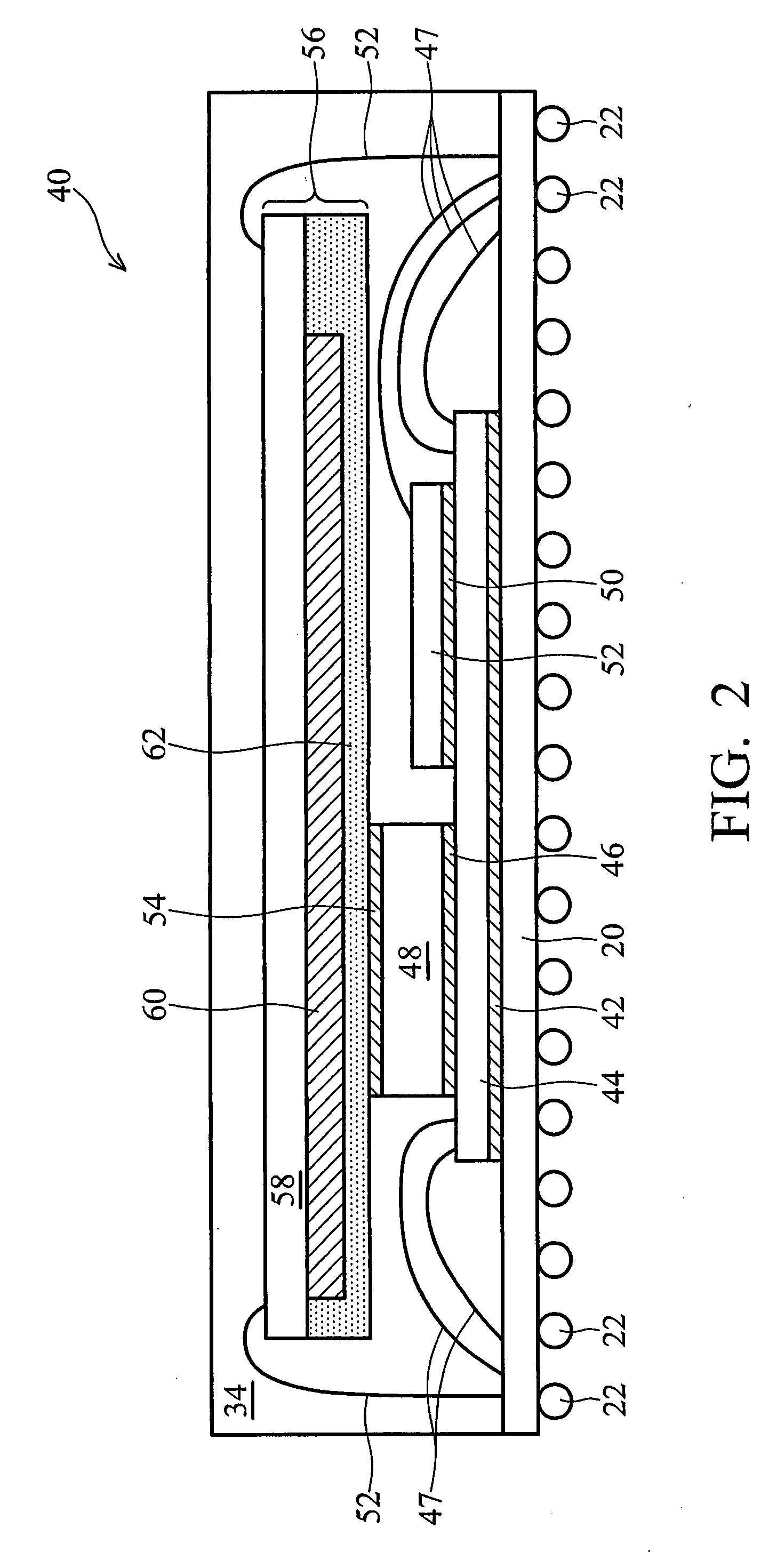
[0025]FIG. 2 illustrates the present invention. Package 40 includes at least one die and at least one package module, and thus has a package-in-package structure. In this embodiment, wire bonding is used to attach dies to package substrate 20. BGA balls 22 are mounted on package substrate 20, and are electrically connected to the dies through the wire bonding. In an exemplary embodiment, a stack die structure, which includes a first die 44 and a second die 52, is packaged. The first die 44 is attached to package substrate 20 through elastic die-attaching film 42. The second die 52 is attached to first die 44 through elastic die-attaching film 50. First die 44 and second die 52 are bonded to package substrate 20 through wires 47. Each of the first die 44 and second die 52 may include digital circuits, analog circuits, and combinations thereof. As is known in the art, analog circuits are prone to the effect of stress, and their performance may shift under the stress. In an exemplary e...

third embodiment

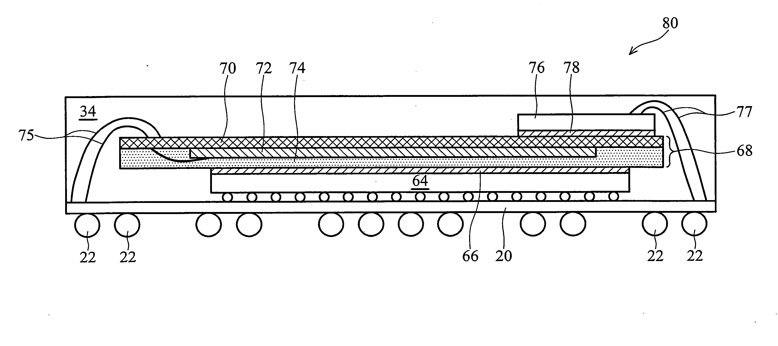
[0029]FIG. 3 illustrates the present invention. Package 80 includes a first die 64 bonded to package substrate 20 through flip-chip bonding. BGA balls 22 are mounted on package substrate 20, and are electrically connected to the first die 64. BGA balls 22 further include portions connected to other dies and packages, such as package module 68 and die 76, through wire bonding.

[0030]Package module 68 includes package substrate 70, die 72 and molding compound 74. Wires 75 connect package module 68 to package substrate 20. In an exemplary embodiment, die 72 is a memory die including, for example, static random access memories. Package module 68 is attached to first die 64 through elastic die-attaching film 66.

[0031]A second die 76 is attached to package module 68 through elastic die-attaching film 78, wherein the second die 76 is bonded to package substrate 70 through wires 77. Similar to the second embodiment, each of the first die 64 and second die 76 may include digital circuits, ana...


PUM


Abstract

A semiconductor package structure is provided. The semiconductor package structure includes a first module; a second module, wherein the first and the second modules each are selected from the group consisting essentially of a package substrate, a die and a package module; and an elastic die-attaching film having a hardness of less than about 150 MPa interposed between the first and the second modules.

Description

TECHNICAL FIELD[0001]This invention relates generally to the packaging of semiconductor dies, and more particularly to the packaging materials and methods for reducing stresses in packages.BACKGROUND[0002]The fabrication of modern circuits typically includes several steps. Integrated circuits are first fabricated on a semiconductor wafer, which contains multiple identical semiconductor chips (also referred to as dies in the packaging art), each comprising integrated circuits. The semiconductor dies are then sawed from the wafer and packaged. The packaging processes have two main purposes: to protect delicate semiconductor dies and to connect interior integrated circuits in the dies to exterior pins of the packages.[0003]In conventional packaging processes, semiconductor dies are mounted on a package substrate using flip-chip bonding or wire bonding. An epoxy molding compound is interposed between dies and the package substrate, and between dies. The epoxy molding compound is used to...

Claims


Application Information

Patent Timeline
IPC IPC(8): H01L23/48
CPCH01L25/03H01L2224/73253H01L2224/16225H01L2224/48091H01L2224/48227H01L2224/73265H01L2225/0651H01L2225/06513H01L2225/06562H01L25/0657H01L2924/15311H01L2924/19107H01L2224/73204H01L2224/32225H01L2224/32145H01L2924/01322H01L2924/01019H01L2924/00014H01L2924/00H01L2924/00012H01L24/73H01L2224/73215H01L2924/00011H01L2924/14H01L2224/0401
Inventor SU, CHAO-YUAN
Owner TAIWAN SEMICON MFG CO LTD
Why Eureka
Try Eureka