

Liquid crystal display panel modules
a technology module, which is applied in the field of liquid crystal display panel module, can solve the problems of inability to achieve optimal modulation of red, green and blue gamma curves
- Summary
- Abstract
- Description
- Claims
- Application Information
AI Technical Summary
Benefits of technology
Problems solved by technology
Method used
Image

Examples
first embodiment
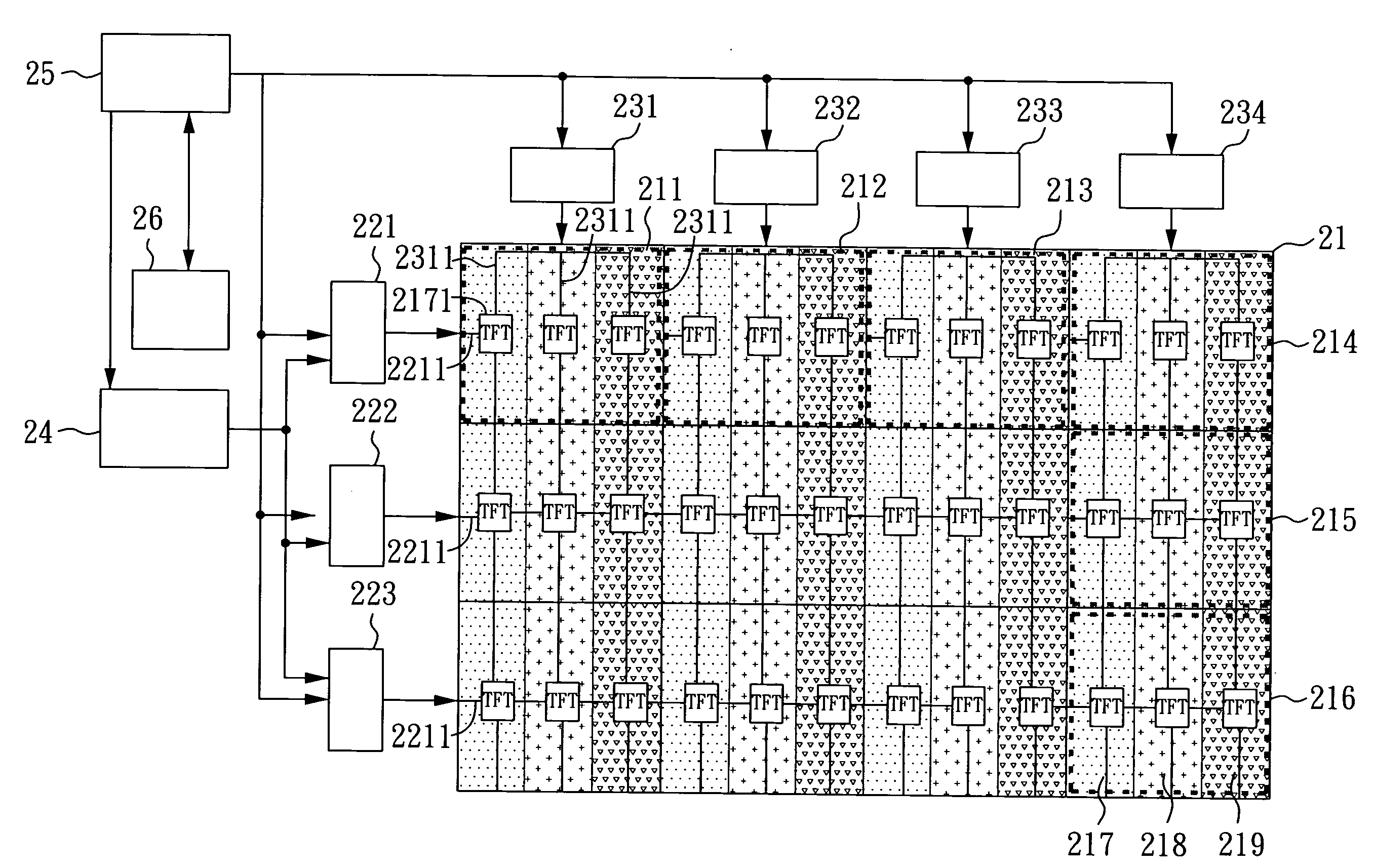
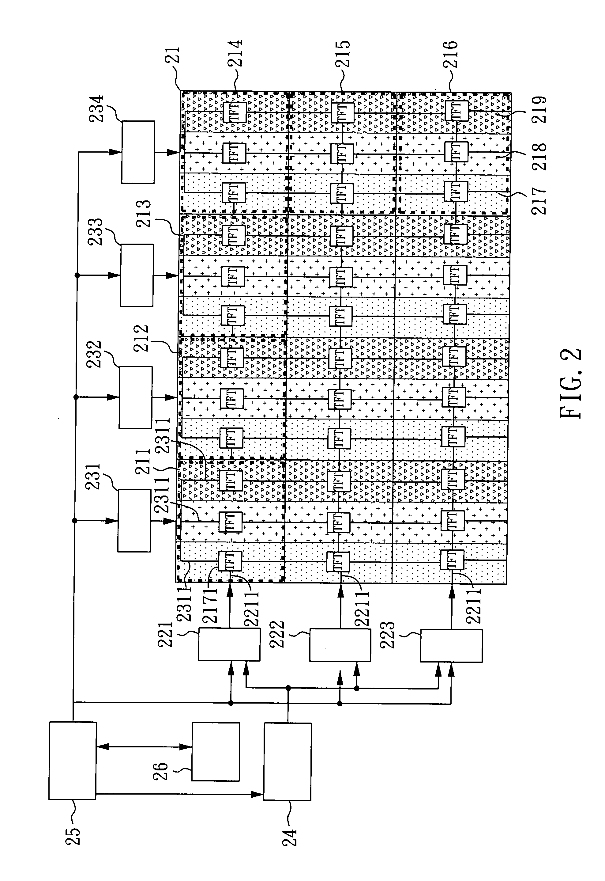
[0045]FIG. 2 is a function block diagram for an LCD panel module according to the present invention, wherein the LCD panel module comprises an LCD display panel 21, a plurality of gate drivers 231, 232, 233, 234, a plurality of source drivers 221, 222, 223, a gamma reference voltage generator 24, a timing controller 25, and a storage device 26. The LCD display panel 21 comprises a plurality of display areas 211, 212, 213, 214, 215, 216 each of which has a red display sub-area 217, a green display sub-area 218 and a blue display sub-area 219, respectively, wherein each of the display sub-areas 217, 218, 219 has a thin film transistor 2171 connected to the gate drivers 231, 232, 233, 234 through gate lines 2211 and connected to the source drivers 221, 222, 223 through source lines 2311. The layout of the thin film transistor 2171, gate lines 2211, and source lines 2311 may vary due to variable considerations, however, the present embodiment merely offers an example of the layouts.
[004...
second embodiment
[0059]the present invention will be described with reference to FIGS. 4A and 4B, in which FIG. 4A is a schematic view illustrating an LCD panel module. The LCD panel module comprises a display panel 41, a plurality of gate drivers 421, 422, 423, a plurality of source drivers 431, 432, 433, 434, a gamma reference voltage generator 44, and a timing controller 45. The display panel 41 comprises a plurality of display areas 411, 412, 413, 414, 415, 416 each of which has a red display sub-area 417, a green display sub-area 418 and a blue display sub-area 419, wherein each of the display sub-areas 417, 418, 419 has a thin film transistor 4171 connected to the gate drivers 421, 422, 423 through source lines 4311 and connected to the source drivers 431, 432, 433, 434 through gate lines 4211. The layout of the thin film transistor 4171, gate lines 4211, and source lines 4311 may vary due to variable considerations, however, the present embodiment merely offers an example of the layouts.
[0060...
third embodiment
[0074]the present invention, providing a timing controller for outputting single-color display data groups to the source drivers, will be described with reference to FIGS. 6A and 6B. FIG. 6A is a schematic view illustrating an LCD panel module, which comprises a display panel 61, a plurality of gate drivers 621, 622, 623, a plurality of source drivers 631, 632, 633, 634, a gamma reference voltage generator 64, and a timing controller 65. The display panel 61 comprises a plurality of display areas 611, 612, 613, 614, 615, 616 each of which has a red display sub-area 617, a green display sub-area 618 and a blue display sub-area 619, wherein each of the display sub-areas 617, 618, 619 has a thin film transistor 6171 connected to the gate drivers 621, 622, 623 through source lines 6311 and connected to the source drivers 631, 632, 633, 634 through gate lines 6211. The layout of the thin film transistor 6171, gate lines 6211, and source lines 6311 may vary due to variable considerations,...
PUM
 Abstract
Description
Claims
Application Information