

Optical element package
- Summary
- Abstract
- Description
- Claims
- Application Information
AI Technical Summary
Benefits of technology
Problems solved by technology
Method used
Image

Examples
first embodiment
Modification of First Embodiment
[0097]In the foregoing embodiment, the packaging film 20 covers the diffusion plate 11 as the support medium. However, the packaging film 20 may cover other support medium. As other support medium, for example, a transparent plate such as plastic and glass, an optical plate to change light characteristics of light emitted from the light source by providing diffusion, light collection and the like are cited. As the optical plate, for example, a wave plate, a reflective polarizing plate, a prism plate having a concave and convex shape such as a prism or the like is cited. To function as a support medium, the thickness thereof is preferably in the range about from 1000 μm to 10000 μm. Above the light source of a direct-lighting liquid crystal display unit, a resin plate including a diffusion filler being about 1 mm to 4 mm thick having a diagonal diameter of about 2 inches to 100 inches, a diffusion optical plate having a layer provided with a shape as a...
second embodiment
Modification of Second Embodiment
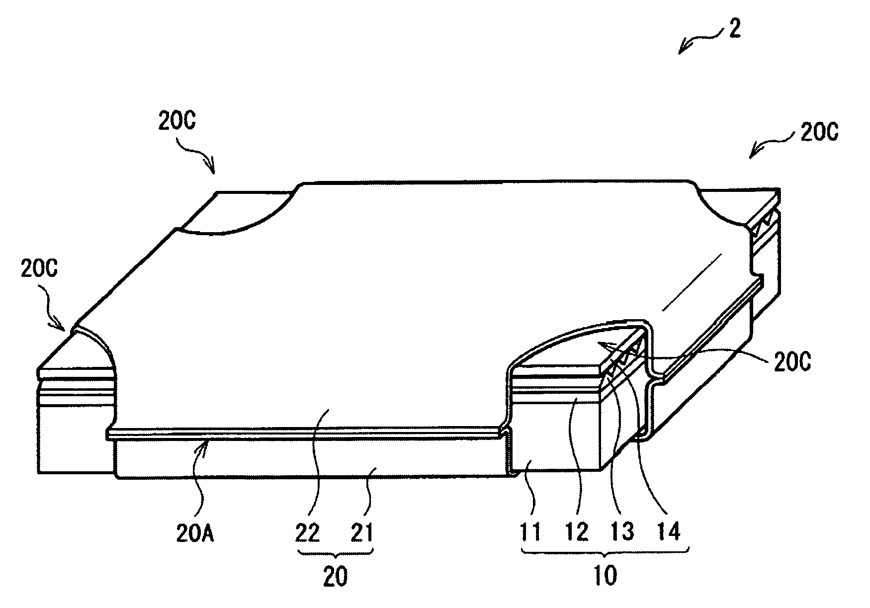
[0111]In the foregoing embodiment, the description has been given of the case that the stack 10 in which the diffusion plate 11, the diffusion sheet 12, the lens film 13, and the reflective polarizing sheet 14 are sequentially layered from the light source image segmentation section 23 side is covered with the packaging film 20 as an example. However, it is possible that an optical sheet having a diffusion function (for example, an optical sheet similar to the diffusion sheet 12) is arranged instead of the reflective polarizing sheet 14.
Third Embodiment
[0112]Next, a description will be given of a third embodiment of the invention.
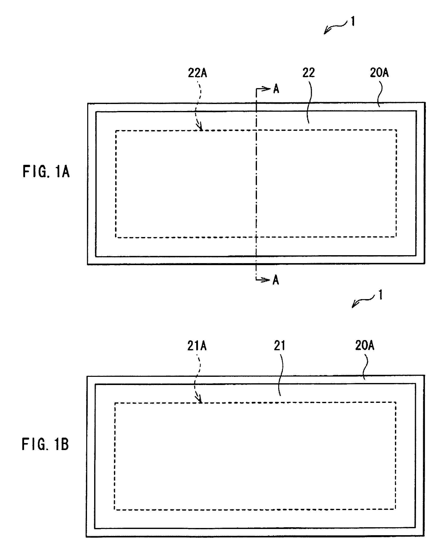
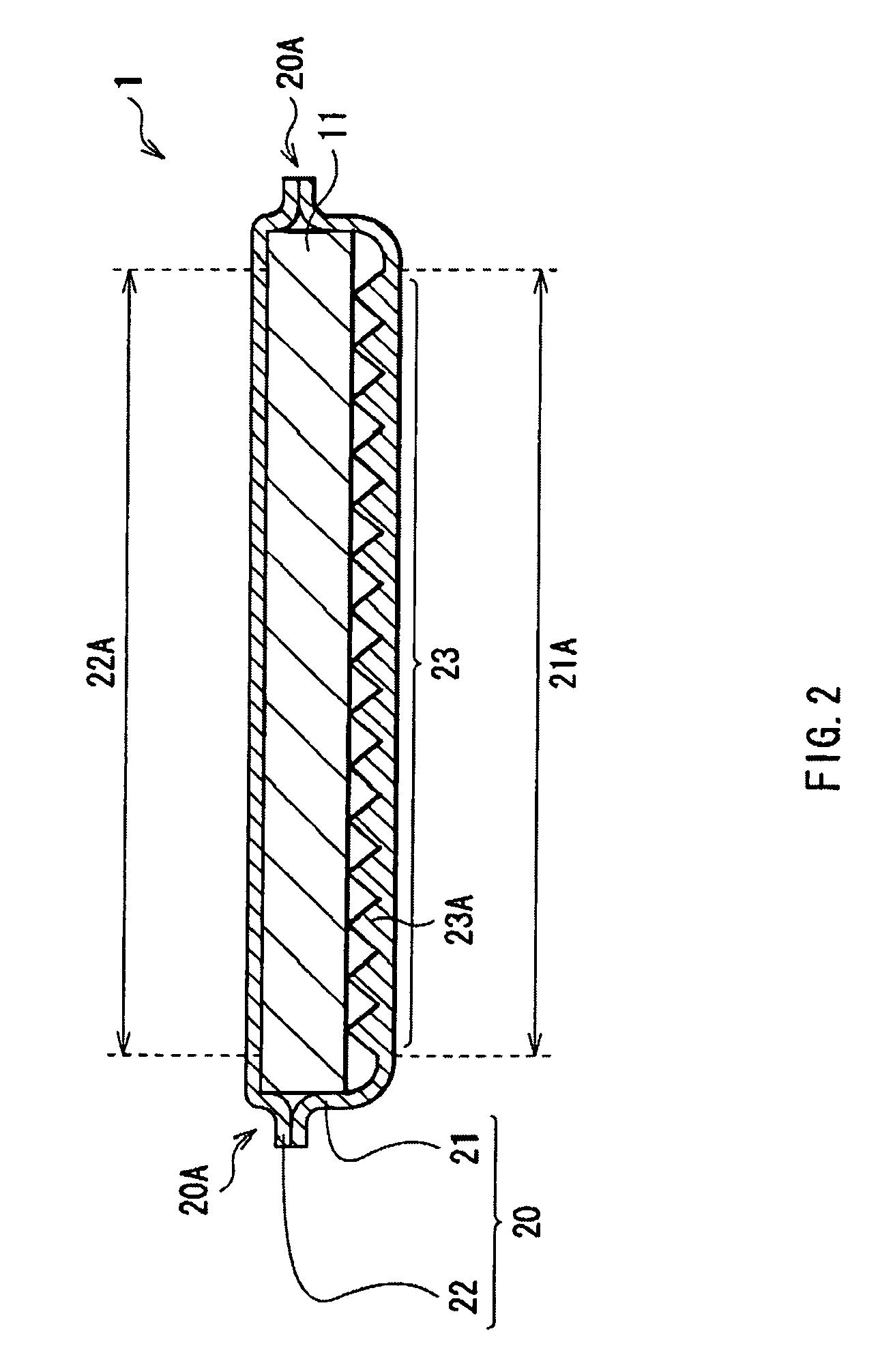
[0113]FIG. 4A shows an example of a top face structure of an optical packaged body 3 according to the third embodiment of the invention. FIG. 4B shows an example of a bottom face structure of the optical packaged body 3 of FIG. 4A. FIG. 5 shows an example of a cross sectional structure taken along arrow A-A of the optical pa...
third embodiment
Modification of Third Embodiment
[0149]In the foregoing embodiment, the description has been given of the case that the stack 10 in which the light source image segmentation sheet 15, the diffusion plate 11, and the diffusion sheet 12 are sequentially layered toward the polarization split section 24 is covered with the packaging film 20 as an example. However, for example, as shown in FIG. 12, the lens film 13 may be arranged between the diffusion sheet 12 and the polarization split section 24. At this time, each convex section 13A of the lens film 13 preferably extends in the short direction of the diffusion plate 11 (direction orthogonal to the extending direction of the convex section 15A of the light source image segmentation sheet 15 and the convex section 24A of the polarization split section 24). Further, in the foregoing embodiment, the description has been given of the case that each convex section 24A extends in the extending direction of the convex section 15A as an exampl...
PUM
| Property | Measurement | Unit |
|---|---|---|
| Thickness | aaaaa | aaaaa |
| Thickness | aaaaa | aaaaa |
| Force | aaaaa | aaaaa |
Abstract
Description
Claims
Application Information