Light emission device

a technology of light emission and light, which is applied in the direction of semiconductor devices, basic electric elements, electrical appliances, etc., can solve problems such as heat dissipation, and achieve the effect of easy realization of color changes

Active Publication Date: 2008-09-11
IVOCLAR VIVADENT AG
View PDF4 Cites 5 Cited by
  • Summary
  • Abstract
  • Description
  • Claims
  • Application Information

AI Technical Summary

Benefits of technology

[0021]It is particularly favorable if a converging lens is fitted above the topmost semiconductor chip.
[0022]The emitted light radiation can thereby be focused in a suitable manner, it also being readily possible according to the invention for the emitted light to be conducted into an optical waveguide such as a light guiding rod.
[0023]According to the invention, it is preferred for the arrangement of the semiconductor chips to be free of reflectors and reflection layers, apart from a reflection layer arranged below the bottommost semiconductor chip. Said reflection layer reflects the downwardly emitted radiation essentially completely and has an effect upward, it being preferred for the semiconductor chip arrangement to be surrounded by a ring reflector by means of which the radiation reflected in this way is additionally projected toward the front and focused.
[0024]According to the invention it is also readily possible to configure the stacked semiconductor chips such that they emit light in different wavelength ranges. For this purpose, it is possible to make use of the fact that each semiconductor chip is provided with connection areas. The electrical driving can thus be effected independently of one another, such that color changes can also readily be realized.
[0025]According to the invention, in the case of the preferred pyramidal construction of the semiconductor chip arrangement, use is also made of the effect that the bottommost semiconductor chip exhibits the highest light emission and, accompanying this, evolution of heat. The heat arising there can be dissipated very well on account of the direct mounting onto a substrate having a thermal conductivity, while the quantity of heat introduced in the case of semiconductor chips arranged further up is also smaller according to the smaller dimensions of said chips.

Problems solved by technology

A problem in this case, of course, is the heat dissipation, since the closely adjacent arrangement of the semiconductor chips means that the latter become very hot at corresponding power.

Method used


Image

  • Light emission device
  • Light emission device
  • Light emission device

Examples


Embodiment Construction

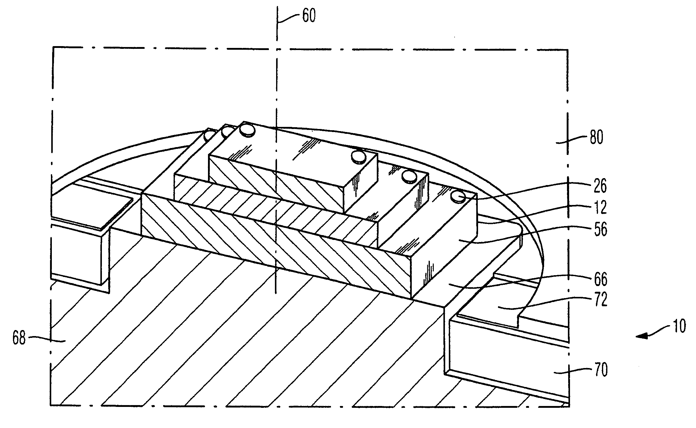
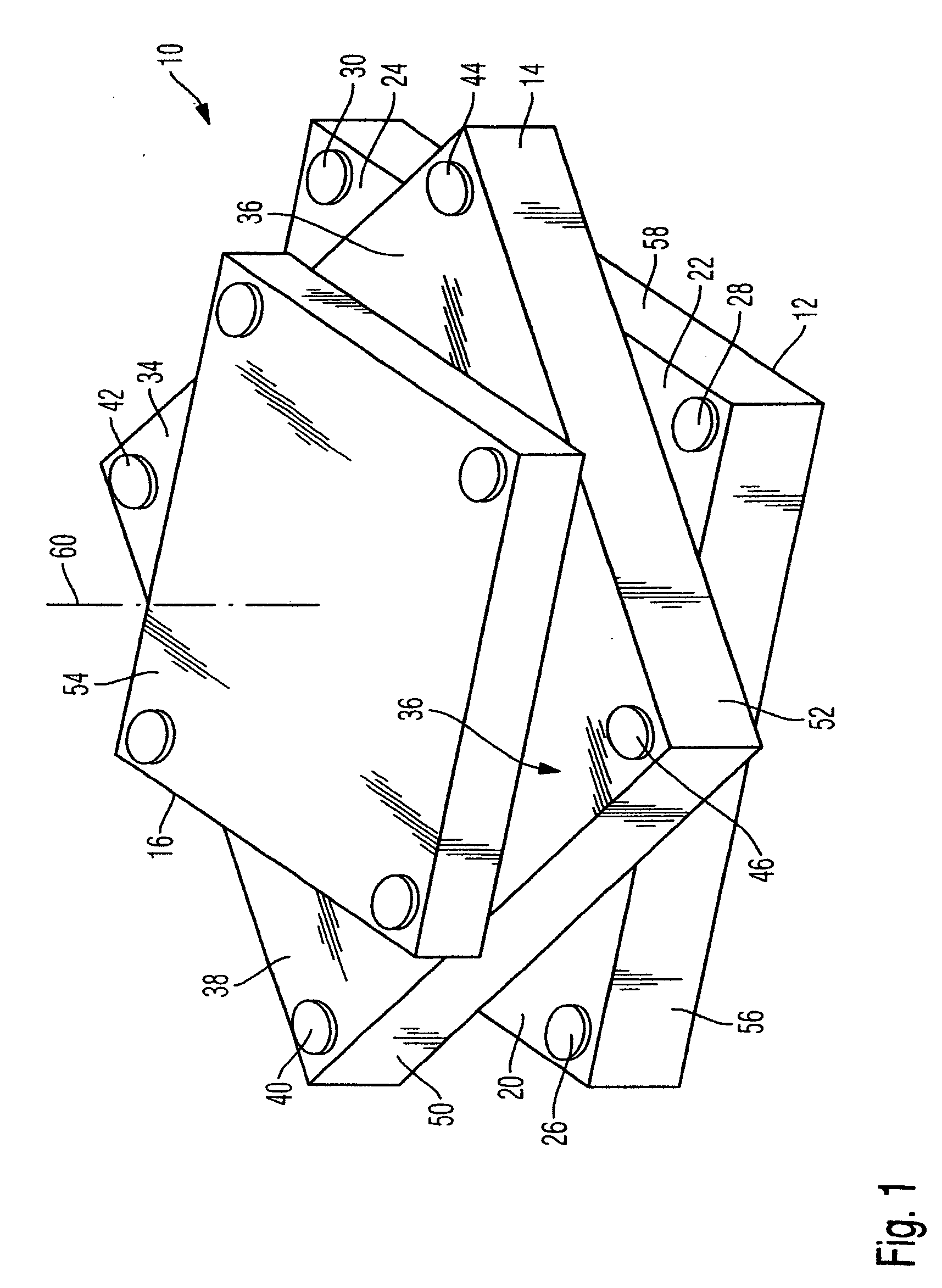
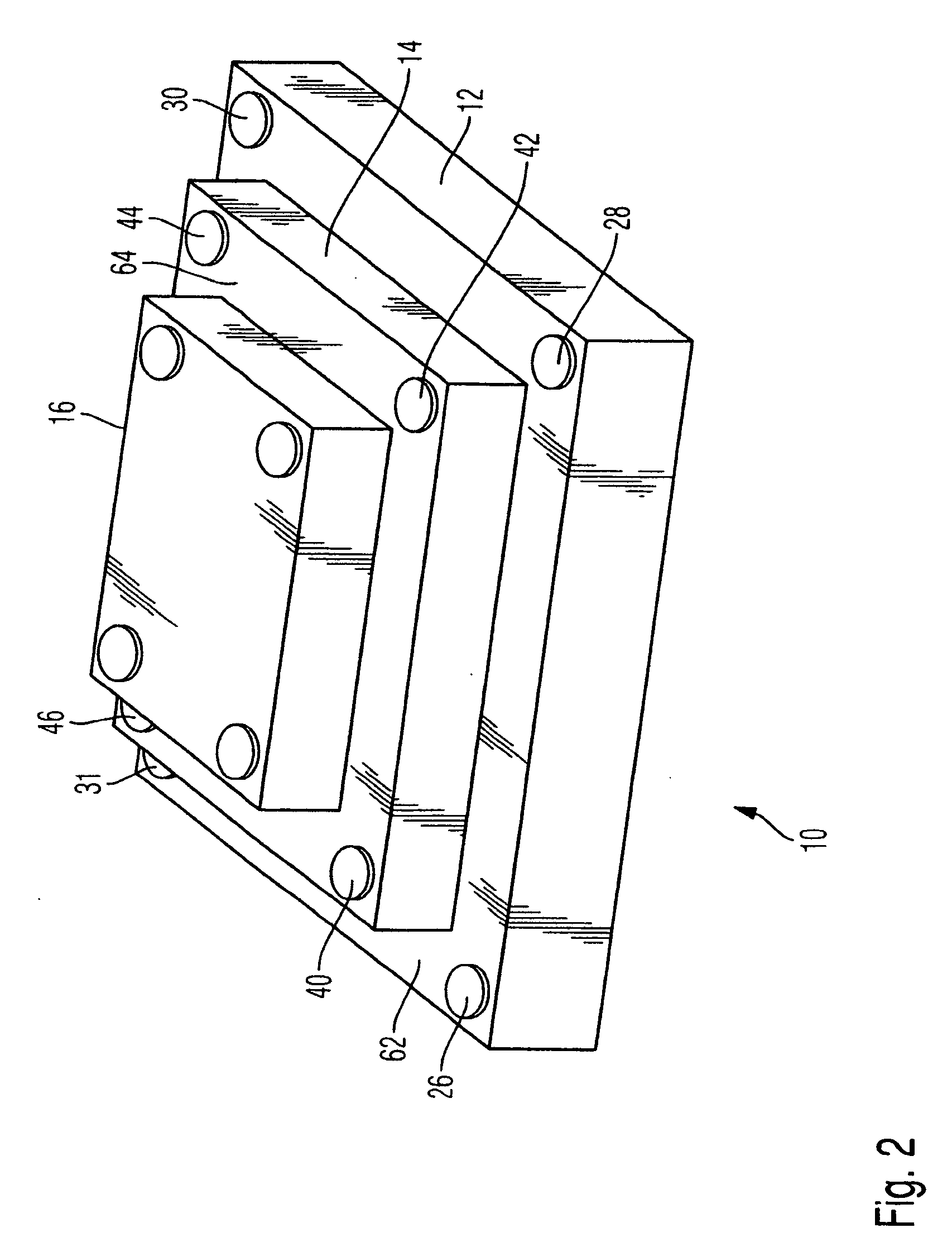
[0054]FIG. 1 reveals a light emission device 10 according to the invention in one embodiment. This light emission device 10 has a plurality of semiconductor chips, namely a lower semiconductor chip 12, a middle semiconductor chip 14 and an upper semiconductor chip 16. In this case, the lower semiconductor chip 12, which may also be referred to as first semiconductor chip, is fitted onto a substrate, which can be seen from FIG. 3 by way of example.

[0055]The substrate may be configured in any suitable manner. It preferably dissipates heat that is particularly preferably metallic. However, it is also possible, in a solution with lower power, to use a plastic casting material as substrate, which then fixes the spatial arrangement of the semiconductor chips.

[0056]In the exemplary embodiment illustrated, the first or lower semiconductor chip 12 is formed as a lamina having an essentially square parallelepiped form. Such semiconductor chips or LED chips are readily commercially available.

[...


PUM


Abstract

The invention relates to a light emission device, comprising at least two light-emitting semiconductor chips and a substrate. At least one first semiconductor chip (12) is fitted on the substrate and a second semiconductor chip (14) is fitted on the first semiconductor chip (12).

Description

CROSS-REFERENCE TO RELATED APPLICATIONS[0001]This application claims priority from U.S. provisional patent application Ser. No. 60 / 931,577 filed May 24, 2007.TECHNICAL FIELD[0002]The present invention relates to a light emission device, comprising at least two light-emitting semiconductor chips and a substrate, at least one first semiconductor chip is fitted on the substrate and a second semiconductor chip is fitted on the first semiconductor chip.BACKGROUND OF THE INVENTION[0003]Numerous attempts have been made to increase the emission intensity of light emitting diodes. It has thus been proposed to arrange a plurality of very small light emitting diode semiconductor chips closely adjacent to one another in order to attain a higher luminous efficiency. A problem in this case, of course, is the heat dissipation, since the closely adjacent arrangement of the semiconductor chips means that the latter become very hot at corresponding power.[0004]It has therefore been attempted to separ...

Claims


Application Information

Patent Timeline
Patent Type & Authority Applications(United States)
IPC IPC(8): H01L33/00H01L33/48H01L33/58H01L33/60
CPCH01L25/0756H01L2225/06562H01L2924/0002H01L2924/00
Inventor PLANK, WOLFGANG
Owner IVOCLAR VIVADENT AG
Why Eureka
Try Eureka