This helps you quickly interpret patents by identifying the three key elements:
Problems solved by technology
Method used
Benefits of technology
[0020]The devices disclosed herein may be combined in various ways within a semiconductor fabrication system, for example to form fabrication facilities adapted to balance processing load among relatively fast and relatively slow processes, or between processes amenable to batch processing and processes that are dedicated to a single wafer.
[0021]In one aspect, a system disclosed herein includes a plurality of process modules coupled together to form a
Problems solved by technology
The complexity of these manufacturing systems continues to grow both due to the increased complexity of processing larger wafers with smaller features, and due to the increasing possibilities for using a single system for several different end-to-end processes, as described for example in commonly-owned U.S. application Ser. No. 11/679,829 filed on Feb. 27, 2007.
As the complexity of a fabrication system grows, it becomes increasingly difficult to schedule resources within the system in a manner that maintains good utilization of all the various process modules.
While a part of this difficulty flows from the complexity of the processing recipe itself, another part of the difficulty comes from the differences in processing time for various processing steps
Method used
Image
Click on the blue label to locate the original text in one second.
Reading with bidirectional positioning of images and text.
Examples
Embodiment Construction
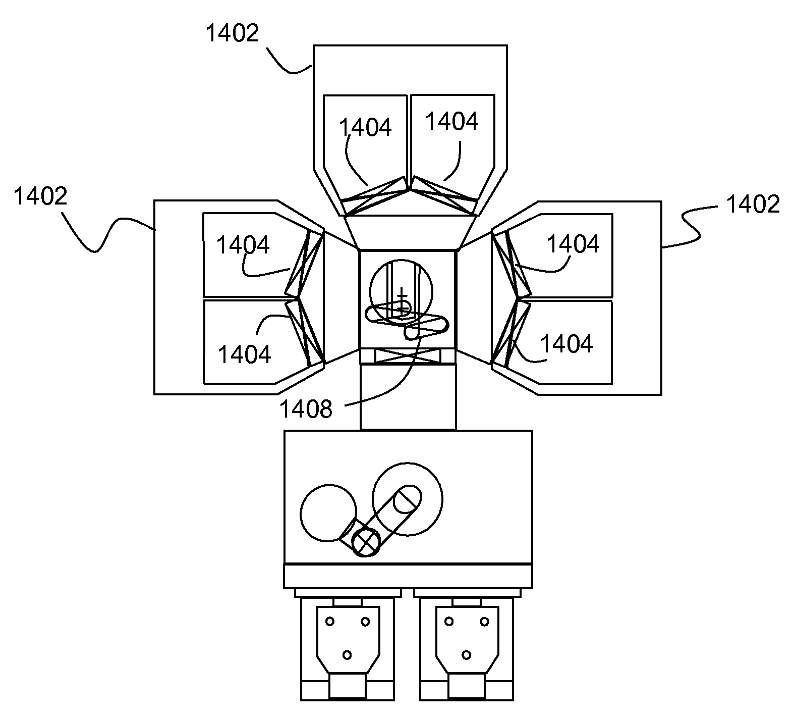
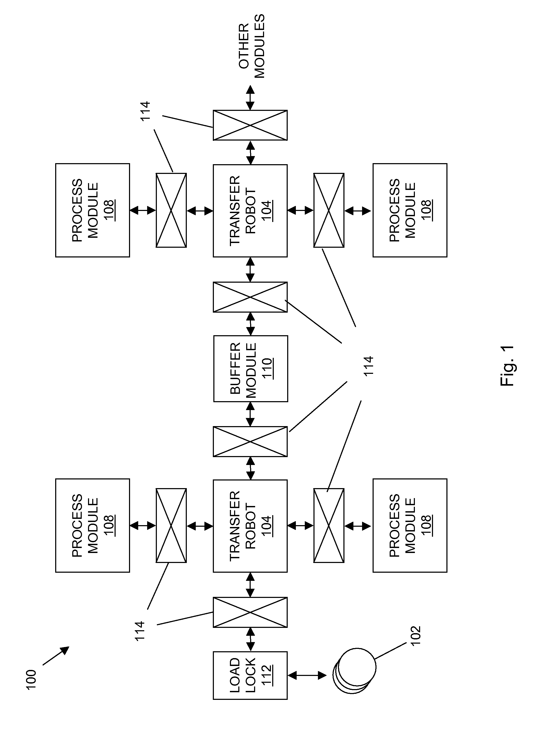
[0046]FIG. 1 shows a generalized layout of a semiconductor manufacturing system. The system 100 may include one or more wafers 102, a load lock 112, one or more transfer robots 104, one or more process modules 108, one or more buffer modules 110, and a plurality of slot valves 114 or other isolation valves for selectively isolated chambers of the system 100, such as during various processing steps. In general operation, the system 100 operates to process wafers for use in, for example, semiconductor devices.
[0047]Wafers 102 may be moved from atmosphere to the vacuum environment through the load lock 112 for processing by the process modules 108. It will be understood that, while the following description is generally directed to wafers, a variety of other objects may be handled within the system 100 including a production wafer, a test wafer, a cleaning wafer, a calibration wafer, or the like, as well as other substrates (such as for reticles, magnetic heads, flat panels, and the li...
PUM
Abstract
A variety of process modules are described for use in semiconductor manufacturing processes.
Description
CROSS-REFERENCE TO RELATED APPLICATIONS[0001]This application is a continuation-in-part of U.S. application Ser. No. 11 / 679,829 filed on Feb. 27, 2007, which claims the benefit of U.S. Prov. App. No. 60 / 777,443 filed on Feb. 27, 2006, and is a continuation-in-part of U.S. application Ser. No. 10 / 985,834 filed on Nov. 10, 2004 which claims the benefit of U.S. Prov. App. No. 60 / 518,823 filed on Nov. 10, 2003 and U.S. Prov. App. No. 60 / 607,649 filed on Sep. 7, 2004.[0002]This application also claims the benefit of the following U.S. applications: U.S. Prov. App. No. 60 / 779,684 filed on Mar. 5, 2006; U.S. Prov. App. No. 60 / 779,707 filed on Mar. 5, 2006; U.S. Prov. App. No. 60 / 779,478 filed on Mar. 5, 2006; U.S. Prov. App. No. 60 / 779,463 filed on Mar. 5, 2006; U.S. Prov. App. No. 60 / 779,609 filed on Mar. 5, 2006; U.S. Prov. App. No. 60 / 784,832 filed on Mar. 21, 2006; U.S. Prov. App. No. 60 / 746,163 filed on May1, 2006; U.S. Prov. App. No. 60 / 807,189 filed on Jul. 12, 2006; and U.S. Prov. ...
Claims
Application Information
Patent Timeline
Application Date:The date an application was filed.
Publication Date:The date a patent or application was officially published.
First Publication Date:The earliest publication date of a patent with the same application number.
Issue Date:Publication date of the patent grant document.
PCT Entry Date:The Entry date of PCT National Phase.
Estimated Expiry Date:The statutory expiry date of a patent right according to the Patent Law, and it is the longest term of protection that the patent right can achieve without the termination of the patent right due to other reasons(Term extension factor has been taken into account ).
Invalid Date:Actual expiry date is based on effective date or publication date of legal transaction data of invalid patent.
IPC IPC(8): H01L21/677
CPCH01L21/67161H01L21/6719H01L21/67184
Inventor VAN DER MEULEN, PETERKILEY, CHRISTOPHER C.PANNESE, PATRICK D.