Method for forming a photoresist-laminated substrate, method for plating an insulating substrate, method for surface treating of a metal layer of a circuit board, and method for manufacturing a multi layer ceramic condenser using metal nanoparticles aerosol

a technology of photoresist and substrate, which is applied in the direction of liquid/solution decomposition chemical coating, railway signalling, chemical coating, etc., can solve the problems of environmental harm, moisture and residual materials are hardly eliminated, and the conventional method of manufacturing a printed circuit board including the step of electroless plating

Active Publication Date: 2008-09-11
SAMSUNG ELECTRO MECHANICS CO LTD
View PDF7 Cites 15 Cited by
  • Summary
  • Abstract
  • Description
  • Claims
  • Application Information

AI Technical Summary

Problems solved by technology

However, this kind of etching method has a problem which moisture and residual materials are hardly eliminated during the peeling process.
Also, the conventional method for manufacturing a printed circuit board including the step of electroless plating and electro plating can be environmental harming because of using the wet plating process.

Method used


Image

  • Method for forming a photoresist-laminated substrate, method for plating an insulating substrate, method for surface treating of a metal layer of a circuit board, and method for manufacturing a multi layer ceramic condenser using metal nanoparticles aerosol
  • Method for forming a photoresist-laminated substrate, method for plating an insulating substrate, method for surface treating of a metal layer of a circuit board, and method for manufacturing a multi layer ceramic condenser using metal nanoparticles aerosol
  • Method for forming a photoresist-laminated substrate, method for plating an insulating substrate, method for surface treating of a metal layer of a circuit board, and method for manufacturing a multi layer ceramic condenser using metal nanoparticles aerosol

Examples


Embodiment Construction

[0033]Hereinafter, according to the present invention, the method for forming photoresist-laminated substrate, method for plating insulating substrate, method for surface treating metal layer of circuit board, and method for manufacturing multi layer ceramic condenser using metal nanoparticles aerosol will be described in detail.

[0034]FIGS. 3A to 3D are schematic diagrams illustrating a method of forming a photoresist-laminated substrate according to one embodiment of the present invention.

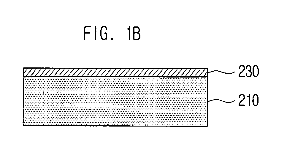
[0035]Illustrating with FIGS. 3A to 3D, a method for forming a photoresist-laminated substrate according to an aspect of the invention includes: preparing a laminated substrate having an insulating substrate 310 and a metal layer 330; coating with an aerosol of metal nanoparticles 350 on the metal layer 330; and laminating a photoresist film 370 on the metal layer 330 coated with the aerosol of metal nanoparticles 350.

[0036]As the invention is for improving the adhesion between the metal layer and...


PUM

PropertyMeasurementUnit
diameteraaaaaaaaaa
thicknessaaaaaaaaaa
thicknessaaaaaaaaaa

Abstract

The present invention relates to a method for forming a photoresist-laminated substrate including: preparing a laminated substrate having an insulating substrate and a metal layer; coating with an aerosol of metal nanoparticles on the metal layer; laminating a photoresist film on the metal layer coated with the aerosol of metal nanoparticles. The method of the present invention is a environmentally friendly method since an aerosol of metal nanoparticles is used, differentiated from the conventional wet process.

Description

CROSS-REFERENCE TO RELATED APPLICATION[0001]This application claims the benefit of Korean Patent Application No. 10-2007-0022563 filed on Mar. 7, 2007, with the Korea Intellectual Property Office, the contents of which are incorporated here by reference in its entirety.BACKGROUND[0002]1. Technical Field[0003]The present invention relates to a method for forming a photoresist-laminated substrate, a method for plating an insulating substrate, a method for surface treating of a metal layer of a circuit board, and a method for manufacturing a multi layer ceramic condenser, in particular, to a method for forming a photoresist-laminated substrate, a method for plating an insulating substrate, a method for surface treating a metal layer of a circuit board, and a method for manufacturing a multi layer ceramic condenser which can be environmentally friendly with employing the dry process which uses an aerosol of metal nanoparticles.[0004]2. Description of the Related Art[0005]A conventional ...

Claims


Application Information

Patent Timeline
Patent Type & Authority Applications(United States)
IPC IPC(8): H03F7/00B05D5/12
CPCH05K1/0306H05K3/064H05K3/102H05K3/108Y10T156/10H05K2201/0257H05K2203/105H05K2203/1344H05K2203/1476H05K3/382
Inventor CHOI, HEE-SUNGKIM, BAE-KYUNKIM, MI-YANGLEE, SEOUNG-JAE
Owner SAMSUNG ELECTRO MECHANICS CO LTD
Why Eureka
Try Eureka