Semiconductor device

a technology of semiconductor devices and semiconductors, applied in semiconductor devices, semiconductor/solid-state device details, electrical apparatus, etc., to achieve the effect of reducing the plane siz

Inactive Publication Date: 2008-09-25
RENESAS ELECTRONICS CORP
View PDF15 Cites 20 Cited by
  • Summary
  • Abstract
  • Description
  • Claims
  • Application Information

AI Technical Summary

Benefits of technology

[0013]In recent years, area reduction (reduction of a plane size) of a semiconductor device has been required. In order to aim at ...

Problems solved by technology

However, since this enlarges area of the capacitive element...

Method used


Image

  • Semiconductor device
  • Semiconductor device
  • Semiconductor device

Examples


embodiment 1

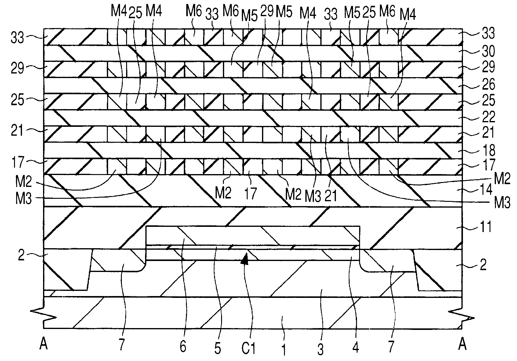
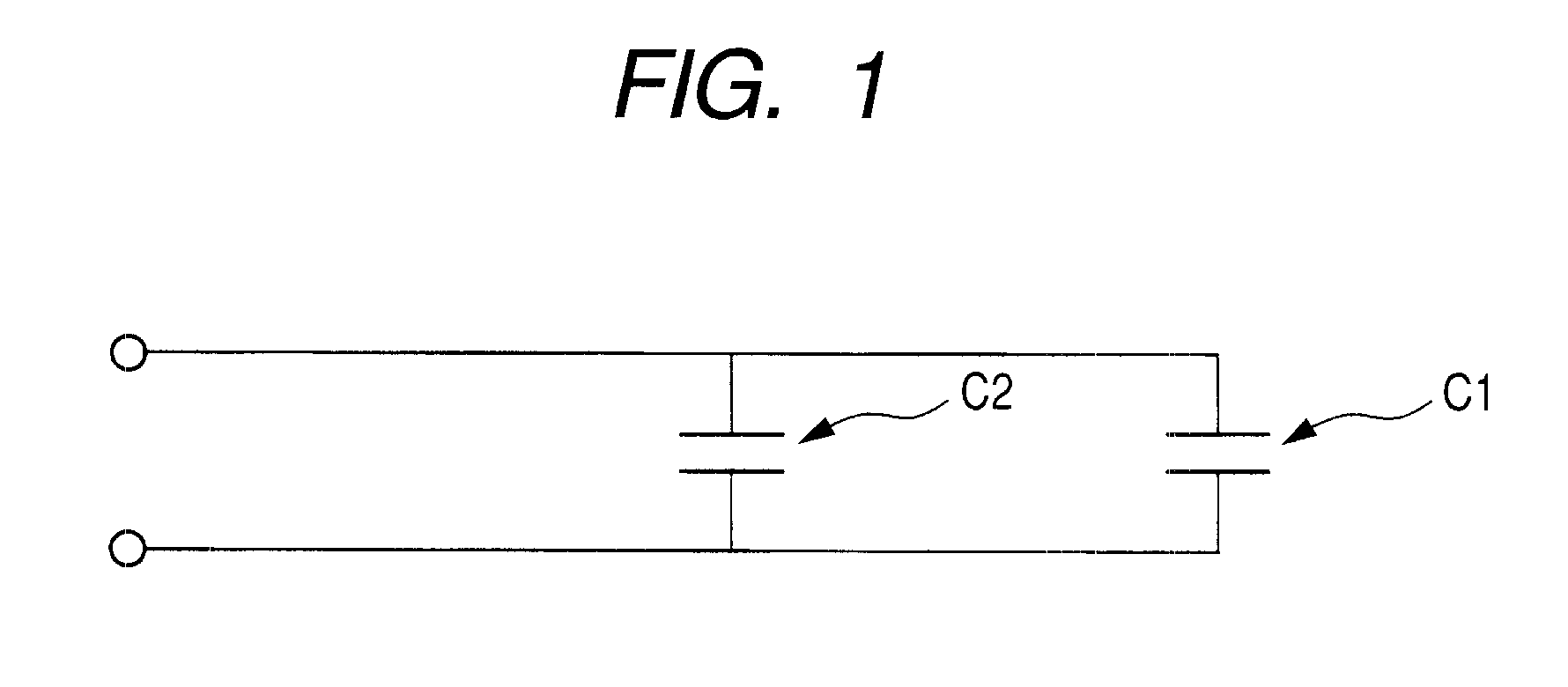
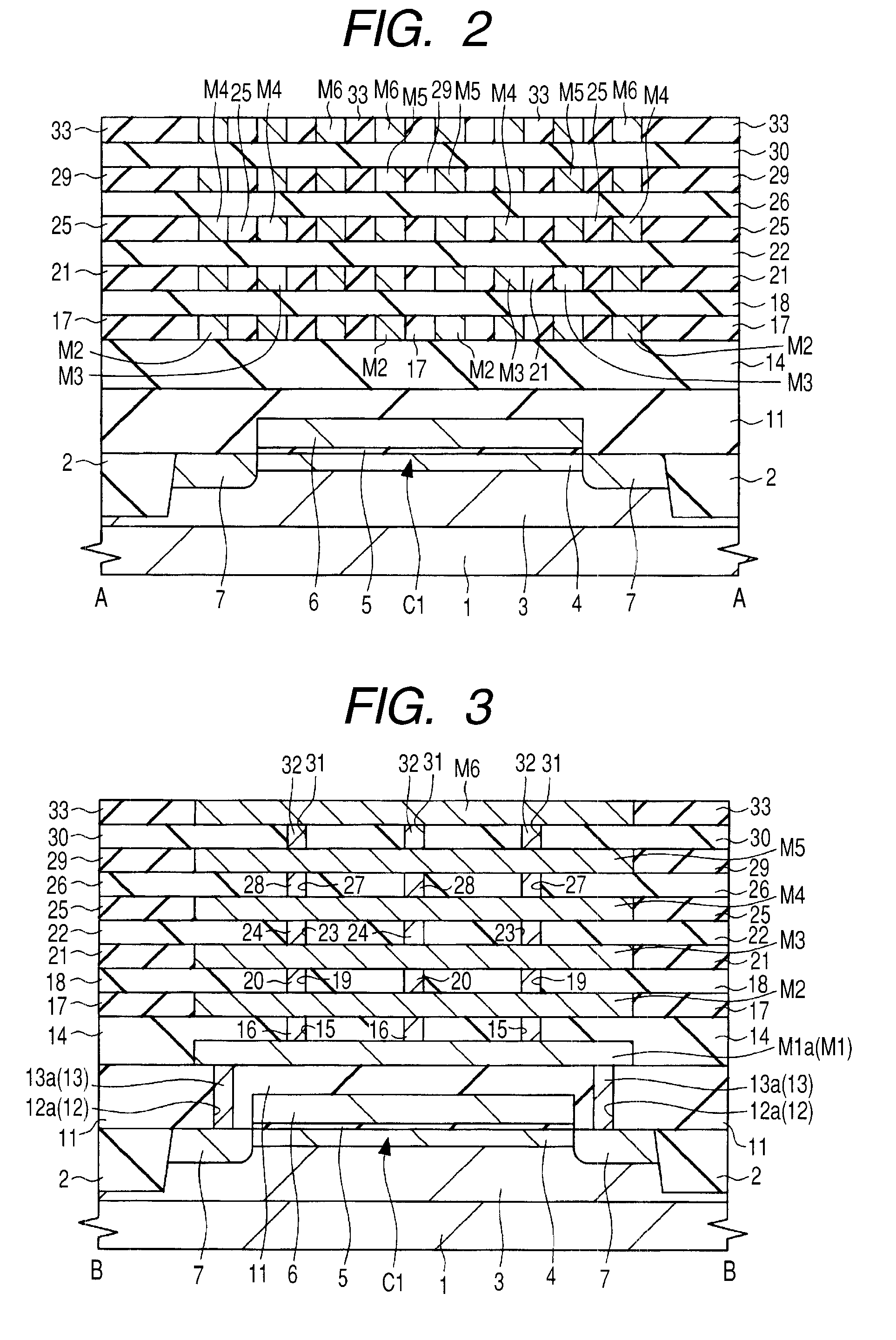
[0048]The semiconductor device of this embodiment is explained with reference to drawings. The semiconductor device of this embodiment is a semiconductor device which has a capacitive element.

[0049]FIG. 1 is a principal part circuit diagram of the semiconductor device of this embodiment, FIG. 2-FIG. 4 are the principal part cross-sectional views of the semiconductor device of this embodiment, and FIG. 5-FIG. 10 are the principal part plan views of the semiconductor device of this embodiment.

[0050]The circuit (equivalent circuit) formed in the capacitor formation region of the semiconductor device shown in FIG. 2-FIG. 10 is shown in FIG. 1. In FIG. 2-FIG. 4, the cross-sectional view of the capacitor formation region of a semiconductor device is shown, and, as for the upper structure than insulation film 33 and wiring M6, illustration is omitted. A different layer of the same plane region (here a capacitor formation region) of a semiconductor device is shown in FIG. 5-FIG. 10. The pla...

embodiment 2

[0118]FIG. 15 is a principal part cross-sectional view of the semiconductor device of this embodiment, and FIG. 16 is a principal part plan view of the semiconductor device of this embodiment. FIG. 15 corresponds to the FIG. 2 of above-mentioned Embodiment 1, and FIG. 16 corresponds to the FIG. 6 of above-mentioned Embodiment 1. Therefore, the section of the A-A line of FIG. 16 corresponds to FIG. 15.

[0119]In this embodiment, as shown in FIG. 15, wiring part MG for a shield which consists of wirings M2-M6 is provided so that wirings (namely, metallic pattern MP1, MP2, MP3, MP4 which were explained by above-mentioned Embodiment 1) M2-M6 which form capacitive element C2 may be surrounded in a capacitor formation region.

[0120]The layout of wiring M2 of a capacitor formation region is shown in FIG. 16. Wiring part MG which consists of wiring M2 is formed so that metallic pattern MP1 and MP2 of wiring M2 may be surrounded in plan view. Wiring part MG is similarly formed with wirings M3-M...

embodiment 3

[0123]FIG. 17 is a principal part circuit diagram of the semiconductor device of this embodiment. FIG. 18 and FIG. 19 are the principal part cross-sectional views of the semiconductor device of this embodiment. FIG. 20 and FIG. 21 are the principal part plan views of the semiconductor device of this embodiment.

[0124]FIG. 17 corresponds to the FIG. 1 of above-mentioned Embodiment 1, and the circuit (equivalent circuit) formed in the capacitor formation region of a semiconductor device shown in FIG. 18-FIG. 21 is shown. As for FIG. 18 and FIG. 19, the cross-sectional view of the capacitor formation region of a semiconductor device is shown, and FIG. 18 corresponds to the FIG. 2 of above-mentioned Embodiment 1. In FIG. 20 and FIG. 21, the same plane position (capacitor formation region) as the FIG. 5-FIG. 10 of above-mentioned Embodiment 1 is shown. The plane layout of wiring M7 which is seventh layer wiring is shown in FIG. 20. Although it is a plan view, in order to make a drawing le...


PUM


Abstract

Coexistence of the realization of high-capacity of a capacitive element and the area reduction of a semiconductor device is aimed at. A plurality of capacitive elements from which a kind differs mutually are accumulated and arranged on a semiconductor substrate, and they are connected in parallel. These capacitive elements are arranged to the same plane region, and make a plane size almost the same. A lower capacitive element is an MOS type capacitive element which uses as both electrodes the n-type semiconductor region formed in the semiconductor substrate, and the upper electrode formed via the insulation film on the n-type semiconductor region. The MIM type capacitive element formed with the pattern of the comb-type of a wiring is arranged in the upper part of a lower capacitive element, and this is connected with a lower capacitive element in parallel.

Description

CROSS-REFERENCE TO RELATED APPLICATION[0001]The present application claims priority from Japanese patent application No. 2007-71836 filed on Mar. 20, 2007, the content of which is hereby incorporated by reference into this application.FIELD OF THE INVENTION[0002]The present invention relates to a semiconductor device, and particularly relates to an effective technology in the application to the semiconductor device which has a capacitive element.DESCRIPTION OF THE BACKGROUND ART[0003]Various semiconductor devices are manufactured by forming MISFET, a capacitor, etc. on a semiconductor substrate and connecting between each element with a wiring.[0004]The technology forming the first MIM capacitance that consists of the first metallic film, the first insulation film, and the first electrode, and the second MIM capacitance that consists of the second metallic film, the second insulation film, and the second electrode on a silicon substrate, and connecting such MIM capacitances in paral...

Claims


Application Information

Patent Timeline
IPC IPC(8): H01L29/94
CPCH01L23/5223H01L29/94H01L2924/0002H01L2924/00H01L27/0805
Inventor MAEDA, SATOSHIHARATA, HIDEHIROKONO, HIROYUKI
Owner RENESAS ELECTRONICS CORP
Why Eureka
Try Eureka