Level shifting circuit and display element driving circuit using same

a level shifting circuit and display element technology, applied in logic circuits, pulse techniques, instruments, etc., can solve the problems of large variation in output electric potential, large chip size, and significant increase, so as to reduce the chip size and the planar dimension of the level shifting circuit.

Inactive Publication Date: 2008-07-08
SHARP KK
View PDF17 Cites 8 Cited by
  • Summary
  • Abstract
  • Description
  • Claims
  • Application Information

AI Technical Summary

Benefits of technology

[0039]Since there is no transition state in which both the first and the second MOS transistors are switched to the ON state at the same time, it is possible to design size of the MOS transistor irrespective of other MOS transistors. Further, there is no longer a need for an element having a long gate-length and / or a wide gate-width, which has been needed in a conventional level shifting circuit. Further, in a case of using an MOS transistor having a large planar dimension for realizing a high-voltage resilience, the level shifting circuit of the present invention only requires two elements (i.e., one P-channel MOS transistor and one N-channel MOS transistor) for performing the level shifting operation and the sampling operation. Thus, it is possible to downsize the planar dimension of the level shifting circuit. Further, when the level shifting circuit is formed into an LSI, the size of the chip can be reduced.
[0040]Thus, it is possible to realize a level shifting circuit whose circuit scale is small.
[0041]Further, the level shifting circuit of the present invention generates no cross-current, and is advantageous in realizing a circuit whose power consumption is low.

Problems solved by technology

Increasing of the gate length and the gate width of these transistors will cause a significant increase in the planar dimension of the circuit, which consequently enlarges the size of a chip, in a case of forming the circuit into an LSI circuit.
If the load capacitor C142 is reduced, the feed-through-caused variation in the output electric potential becomes large, and the retention of the signal becomes difficult.
This is disadvantageous in that the chip size increases in a case of forming the circuit into an LSI.
In conclusion, either of the above described conventional level shifting circuits causes difficulties in reducing the scale of the entire circuit.

Method used


Image

  • Level shifting circuit and display element driving circuit using same
  • Level shifting circuit and display element driving circuit using same
  • Level shifting circuit and display element driving circuit using same

Examples


Embodiment Construction

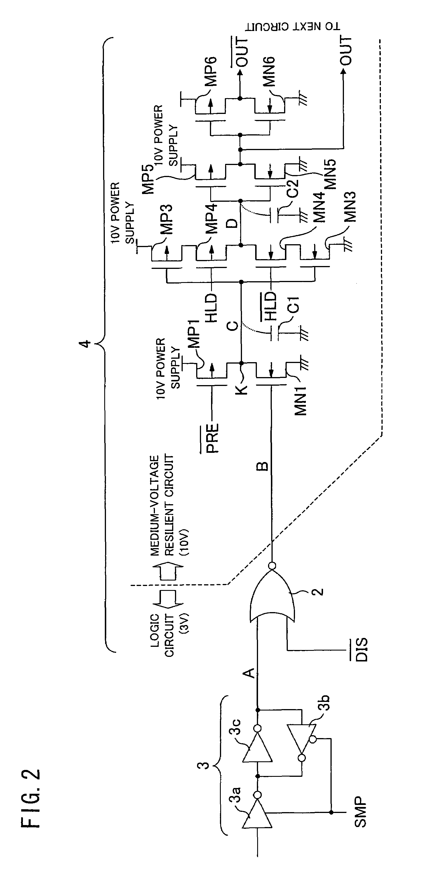
[0053]The following describes an embodiment of the present invention with reference to FIG. 1 through FIG. 3.

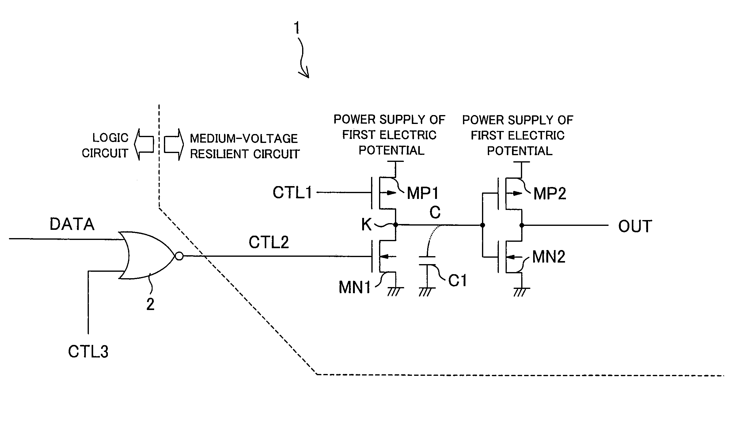
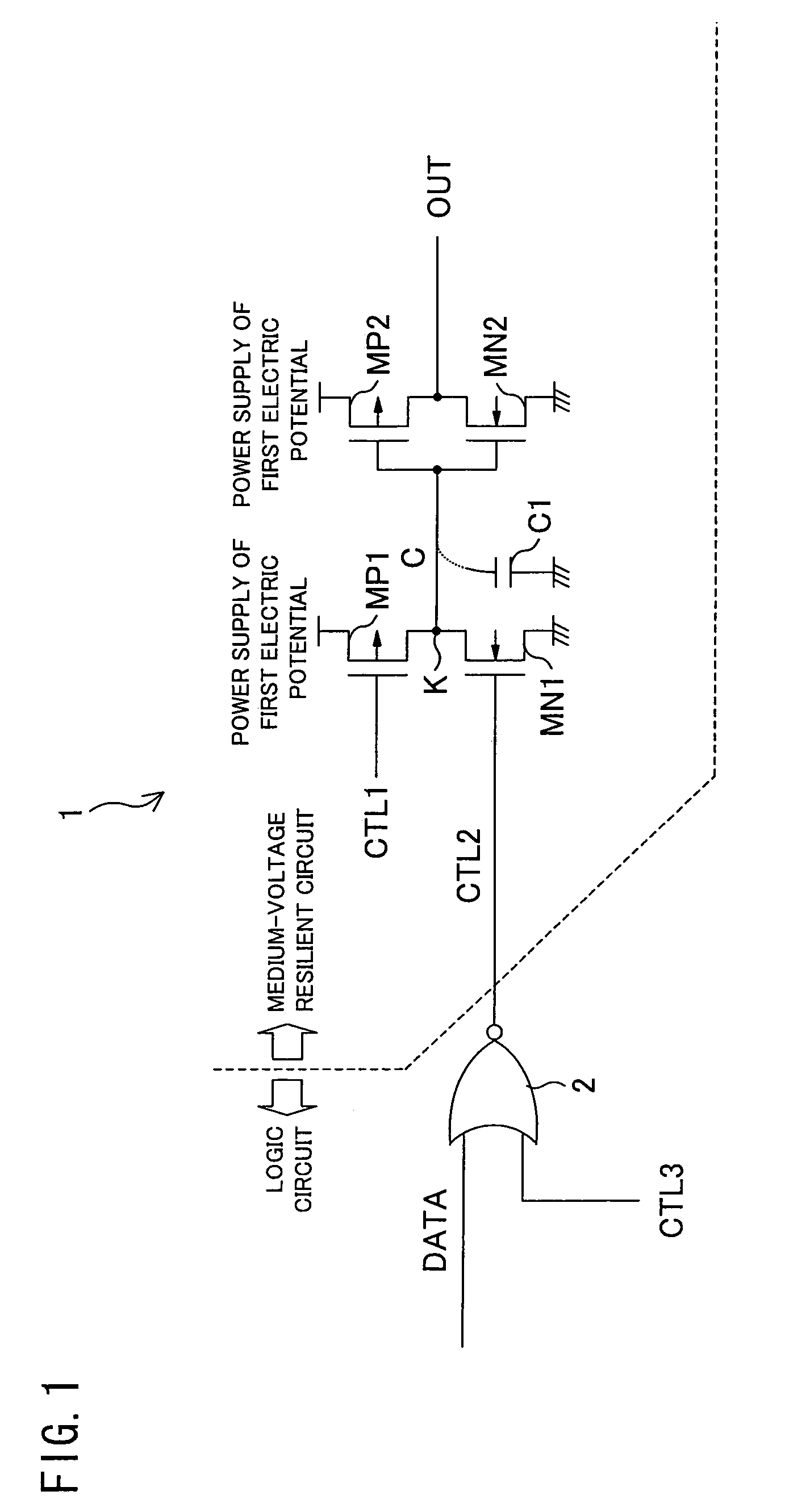
[0054]FIG. 1 illustrates a configuration of a dynamic sampling type level shifting circuit 1 (Hereinafter referred to as level shifting circuit), in accordance with the present embodiment.

[0055]A level shifting circuit 1 includes: P-channel MOS transistors MP1 and MP2; N-channel MOS transistors MN1 and MN2; and a NOR circuit 2.

[0056]The source of the MOS transistor (first MOS transistor) MP1 is connected to a power supply of a first electric potential which is higher than a GND potential. The source of the MOS transistor (second MOS transistor) MN1 is connected to a GND. The drain of the MOS transistor MP1 and the drain of the MOS transistor MN1 are connected with each other, at a connection point-K. A control signal (first control signal) CTL1 is inputted as a gate signal to the gate of the MOS transistor MP1, and a control signal (second control signal) CTL2 is inputted as ...


PUM


Abstract

A P-channel MOS transistor and an N-channel MOS transistor are respectively controlled by a first control signal and a second control signal. The first control signal CTL1 and the second control signal CTL2 are independent from each other. The second control signal CTL2 is generated by a NOR circuit 2 to which a data signal DATA and a third control signal CTL3 are inputted. A load capacitor C1 which samples the first electric potential or the GND electric potential is configured by a gate capacitance of another MOS transistor.

Description

[0001]This Nonprovisional application claims priority under 35 U.S.C. § 119(a) on Patent Application No. 2005 / 023863 filed in Japan on Jan. 31, 2005, the entire contents of which are hereby incorporated by reference.FIELD OF THE INVENTION[0002]The present invention relates to a level shifting circuit, and in particular, the present invention relates to a level shifting circuit having a sampling circuit of a C-MOS configuration, which is needed in a TFT-LCD source driver circuit, for transmitting a digital signal between circuits respectively having different power source voltages.BACKGROUND OF THE INVENTION[0003]In a TFT-LCD source driver circuit in general, a liquid crystal panel is driven as follows. Namely, a display-use signal is digitally processed by a logic circuit which is operated by a power source voltage of approximately 3V. Then, the signal is converted into a voltage of approximately 10V which is required for driving a liquid crystal panel of the TFT-LCD.[0004]FIG. 8 il...

Claims


Application Information

Patent Timeline
Patent Type & Authority Patents(United States)
IPC IPC(8): H03K19/096
CPCG09G3/3685H03K19/01855H03K3/356113G09G3/20G09G2310/027G09G2320/0219G09G2330/021G09G2310/0289G02F1/133H03K19/0175G09G3/36
Inventor NAKAO, TOMOAKI
Owner SHARP KK
Why Eureka
Try Eureka