Delay demodulation devices

a demodulation device and delay technology, applied in the direction of instruments, optical elements, optical waveguide light guides, etc., can solve the problems of reducing the time duration per 1 bit of optical signal, deteriorating communication lines, and difficulty in making a high-speed optical transmission system using existing optical fiber networks, so as to reduce the polarization dependent frequency and reduce the size

Inactive Publication Date: 2011-07-12
FURUKAWA ELECTRIC CO LTD
View PDF9 Cites 7 Cited by
  • Summary
  • Abstract
  • Description
  • Claims
  • Application Information

AI Technical Summary

Benefits of technology

[0009]The present invention seeks to overcome the above-identified problems. The purpose of the present invention is to provide a delay demodulation device with reduced Polarization Dependent frequency and reduced chip size.
[0012]Because reduction in size of a planar lightwave circuit chip is performed, uniformity of the temperature distribution in the surface of a planar lightwave circuit (PLC) can be improved and the shift of center wavelength due to environment and temperature fluctuation can be very small. Also, because reduction in size of a planar lightwave circuit chip is performed, stress distribution within the chip, which causes birefringence, is reduced, and the shift of center wavelength due to the environment and temperature fluctuation can be made very small. Therefore, the delay demodulation device with little or no wavelength shift due to the environment and temperature fluctuation and small initial polarization dependent frequency PDf can be obtained. Furthermore, because the chip is reduced in size, a module using the delay demodulation device can be smaller, and the power consumption of the module can be reduced as well.
[0016]In a delay demodulation device according to the present invention as claimed in 5, the center portion of the two arm-waveguides of the first Mach-Zehnder interferometer are extended in parallel and close to each other, and the center portion of the two arm-waveguides of the second Mach-Zehnder interferometer are extended in parallel and close to each other. According to the construction, retardation of the half wave plate can be suppressed.
[0021]According to the present invention, it becomes able to provide a delay demodulation device in which chip is reduced in size and polarization dependent frequency is reduced.

Problems solved by technology

However, when the transmission rate is increased, the time duration per 1 bit of optical signal is reduced and, because of the characteristics of an optical fiber, signal waveforms are deteriorated, and therefore the quality of a communication line is deteriorated.
Therefore, it is difficult to make a high speed optical transmission system using existing optical fiber networks.
However, in the way of just inserting the half wave plate, it is difficult to lower the Polarization Dependent frequency (PDf) to be less than 0.2 GHz and causes a low yield ratio.
Therefore, it is very difficult to fabricate a delay demodulation circuit with small Polarization Dependent frequency (<0.2 GHz) consistently.

Method used


Image

  • Delay demodulation devices
  • Delay demodulation devices
  • Delay demodulation devices

Examples


embodiment

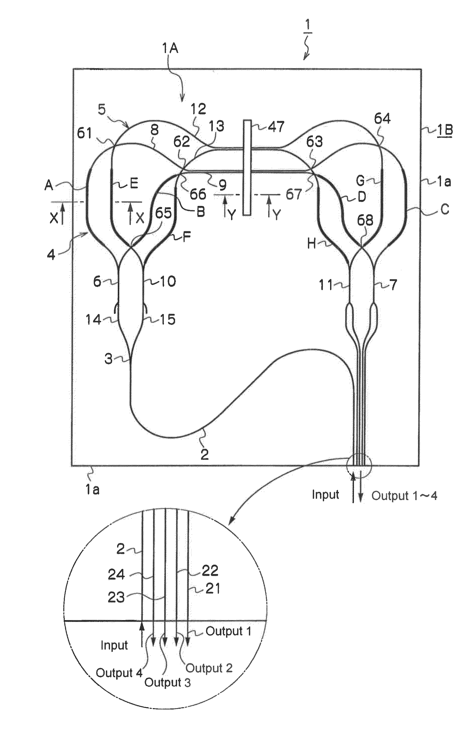
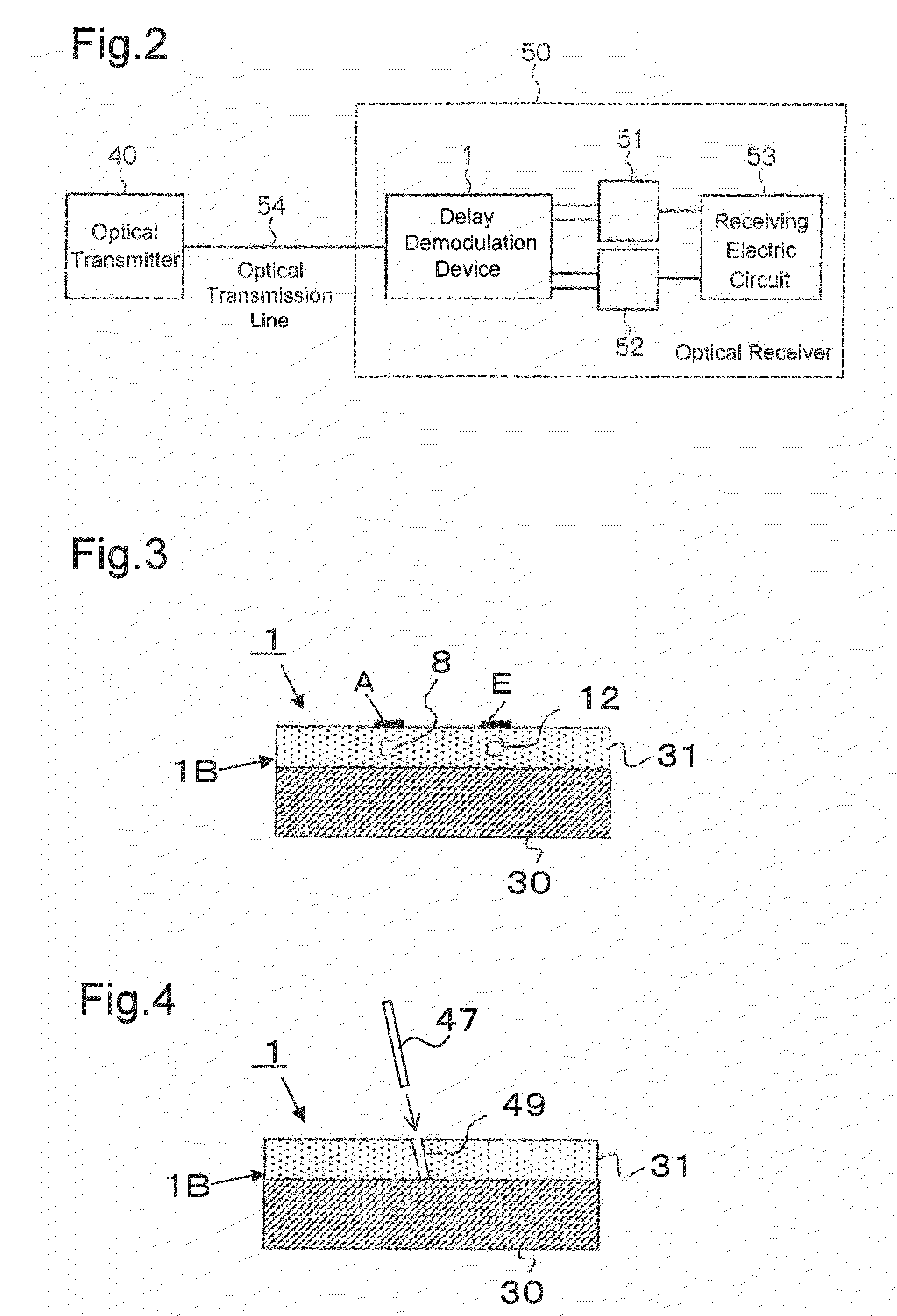
[0055]A delay demodulation device 1 for 40 Gbps DQPSK is fabricated, by forming a planar lightwave circuit (PLC) 1A which includes an input waveguide 2; a Y-branch waveguide 3; Mach-Zehnder interferometers 4, 5; and output waveguides 21˜24 on a silicon base plate 30 shown in FIG. 3, by using FHD method, photolithography and reactive ion etching.

[0056]In the fabricated delay demodulation device 1, in the case of which the difference in the refractive index difference between the cladding layer and the core layer (fractional refractive index difference Δ) is 1.5%, and the size of the circuit (size of the PLC chip 1B) is 19 mm×16 mm and reduction in size is performed. Its FSR is set to 20 GHz. Polarization dependent frequency PDf is adjusted by driving heaters on one of the two Mach-Zehnder interferometers 4, 5. After the adjustment, phase control (phase trimming) is performed by driving heaters on one of the two Mach-Zehnder interferometers 4, 5 to shift the phases of one Mach-Zehnder...


PUM

PropertyMeasurementUnit
Polarization Dependent frequencyaaaaaaaaaa
frequencyaaaaaaaaaa
sizeaaaaaaaaaa

Abstract

The delay demodulation device 1 comprises: an input waveguide 2 which receives DQPSK signals; a Y-branch waveguide 3 which splits the input waveguide 2; a first Mach-Zehnder interferometer 4; and a second Mach-Zehnder interferometer 5. Both end of two arm-waveguides 8, 9 of the first Mach-Zehnder interferometer 4 and both ends of two arm-waveguides 12, 13 of the second Mach-Zehnder interferometer 5 are angled toward the center portion of a planar lightwave circuit (PLC) 1A. Because of the angle, the length of the two arm-waveguides 8, 9 of the first Mach-Zehnder interferometer 4 and the length of the two arm-waveguides 12, 13 of the second Mach-Zehnder interferometer 5 in Z-direction can be shortened, and input couplers 6,10 and output couplers 7,11 of each Mach-Zehnder interferometers in Z-direction can be shortened as well. The area occupied by each Mach-Zehnder interferometers 4, 5 are also reduced.

Description

TECHNICAL FIELD[0001]The present invention relates to a delay demodulation device used for optical fiber communications, and particularly, relates to a delay demodulation device equipped with PLC type-Mach-Zehnder interferometers, which demodulate DQPSK signals in Dense Wavelength Division Multiplexing (DWDM) transmission systems.RELATED ARTS[0002]Recently, with the rapid growth in broadband networks, high speed optical transmission systems (toward transmission rate of 40 Gbps) have been investigated actively. However, when the transmission rate is increased, the time duration per 1 bit of optical signal is reduced and, because of the characteristics of an optical fiber, signal waveforms are deteriorated, and therefore the quality of a communication line is deteriorated. For 40 Gbps-class Long-haul transmission systems, transponders that transform an optical signal to an electrical signal and then transform the electrical signal back to an optical signal are needed in the transmissi...

Claims


Application Information

Patent Timeline
Patent Type & Authority Patents(United States)
IPC IPC(8): H04B10/06G02F2/00G02F1/01H04B10/516H04B10/548H04B10/61
CPCG02B6/12007G02B6/125H04B10/677
Inventor HASEGAWA, JUNICHINARA, KAZUTAKA
Owner FURUKAWA ELECTRIC CO LTD
Why Eureka
Try Eureka