Manufacturing method of semiconductor device and semiconductor device

a manufacturing method and semiconductor technology, applied in the field of semiconductor devices, can solve problems such as contamination of the device region, and achieve the effect of improving the reliability of semiconductor devices

Inactive Publication Date: 2011-06-30
RENESAS ELECTRONICS CORP
View PDF7 Cites 8 Cited by
  • Summary
  • Abstract
  • Description
  • Claims
  • Application Information

AI Technical Summary

Benefits of technology

[0019]The following explains briefly an effect provided by at least one of several embodiments of the invention among those disclosed in the present

Problems solved by technology

However, the surface on the principal surface side of the semiconductor wafer is not a uniformly flat surface, but has roughness following wirings and terminals formed over the principal surface.
Therefore, there occurs such a problem that foreign materials such as grinding waste generated by grinding the back surface side of the semico

Method used


Image

  • Manufacturing method of semiconductor device and semiconductor device
  • Manufacturing method of semiconductor device and semiconductor device
  • Manufacturing method of semiconductor device and semiconductor device

Examples


embodiment 1

Structure of a Semiconductor Chip Semiconductor Device

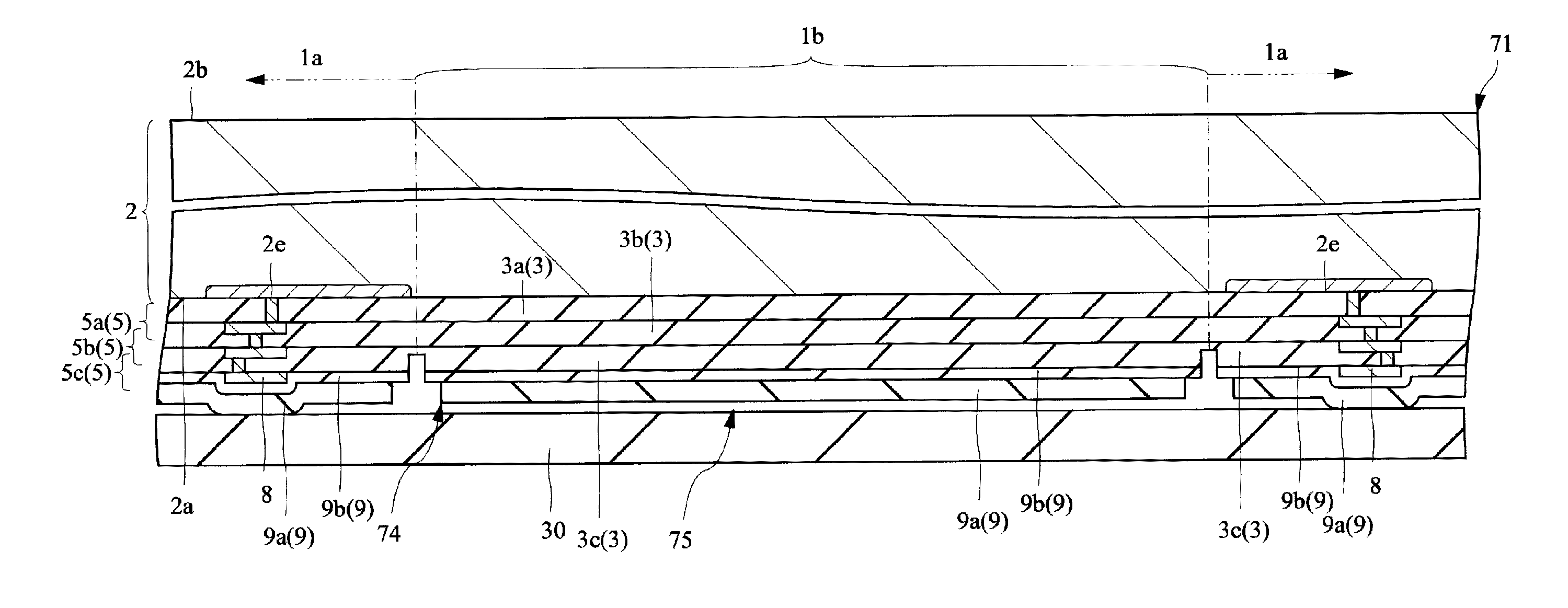
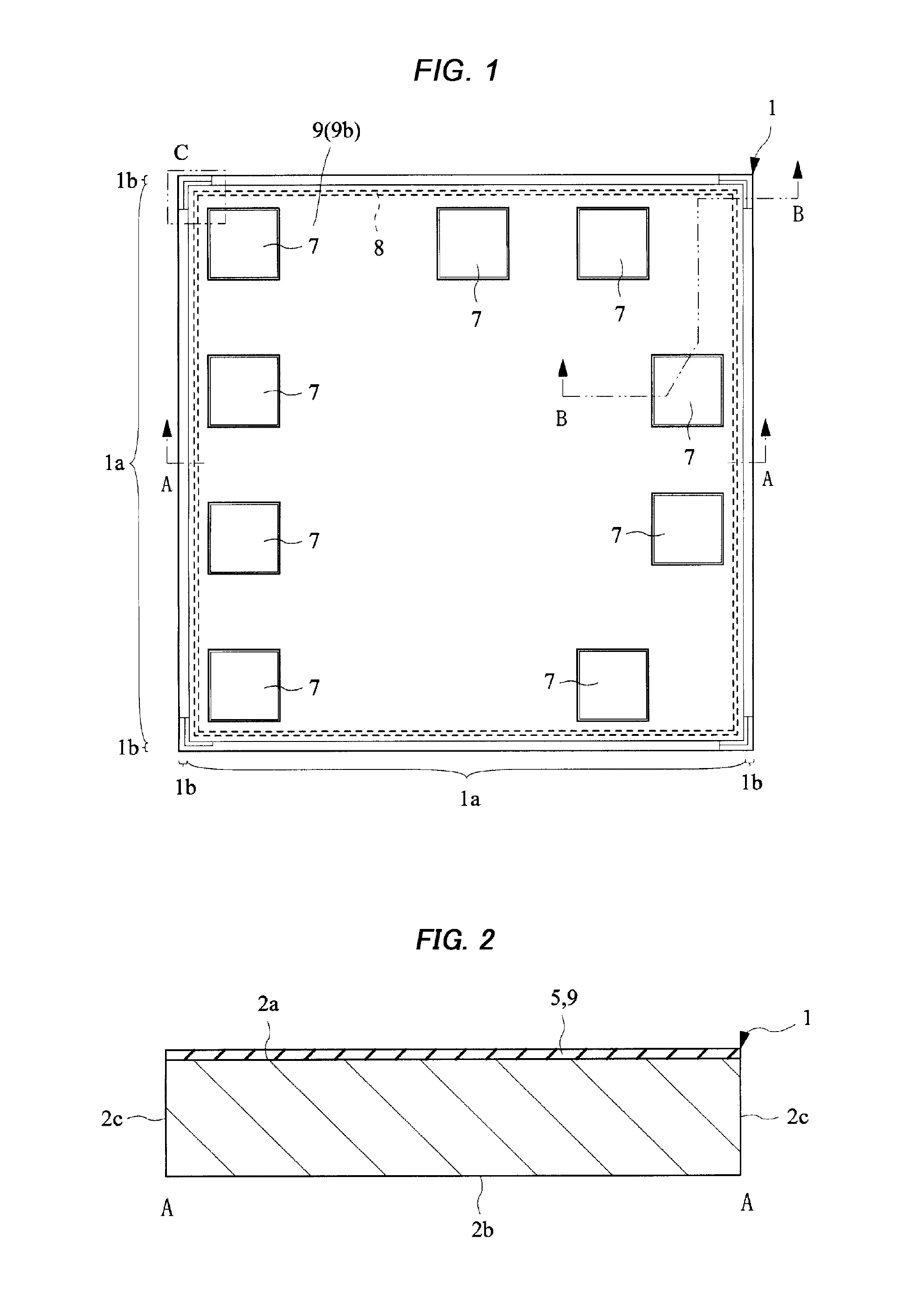
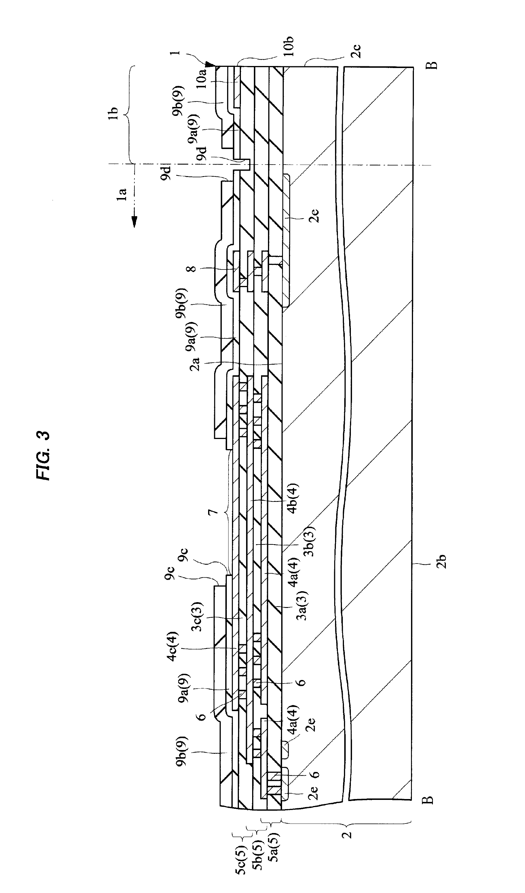
[0056]First, the structure of a semiconductor chip (semiconductor device) according to Embodiment 1 will be explained. FIG. 1 is a plan view showing the principal surface side of a semiconductor chip being a semiconductor device in Embodiment 1. FIG. 2 is a cross-sectional view along the A-A line in FIG. 1, and FIG. 3 is an enlarged cross-sectional view along the B-B line in FIG. 1. FIG. 4 is an enlarged plan view of the C part in FIG. 1. FIGS. 1 and 2 are the plan view and the cross-sectional view respectively showing the overall structure of the semiconductor chip, and the detailed structure of the semiconductor chip is explained using FIGS. 3 and 4, which are enlarged drawings thereof, respectively. Meanwhile, FIG. 4 is a plan view, but hatching is given to make it easy to understand the planar shape of respective insulating layers laminated on the principal surface side, metal patterns etc.

[0057]A semiconductor chip (semicond...

embodiment 2

[0139]In embodiment 1, an embodiment, having an arrangement layout of the stopper 11 over the principal surface 2a of the semiconductor wafer 20 such that the stopper 11 is disposed at each of intersections of plural scribe lines was described. In Embodiment 2, a modified example of the layout of the stopper 11 is described as follows. FIG. 25 is an enlarged plan view showing a part of a semiconductor wafer being a modified example of the semiconductor wafer shown in FIG. 7. Meanwhile, a semiconductor wafer 50 in Embodiment 2 is substantially the same as the wafer in Embodiment 1 except for the layout of the stopper 11. Accordingly, overlapping explanations are omitted with respect to FIGS. 1 to 23 explained in Embodiment 1.

[0140]A difference between the semiconductor wafer 50 in Embodiment 2 shown in FIG. 25 and the semiconductor wafer 20 in Embodiment 1 shown in FIG. 7 lies in the layout of the stopper 11. In more detailed explanation, the semiconductor wafer 50 has plural interse...

embodiment 3

[0148]In Embodiment 1, plural (four) metal patterns 10 are formed for the wiring layer 5c regarding the structure of the stopper 11 over the principal surface 2a of the semiconductor wafer 20. In Embodiment 3, a modified example of the metal pattern to be formed for the stopper 11 is described. FIG. 26 is an enlarged plan view showing a part of a semiconductor wafer being a first modified example of the semiconductor wafer shown in FIG. 9. FIG. 27 is an enlarged plan view showing a part of a semiconductor wafer being a second modified example of the semiconductor wafer shown in FIG. 9. FIG. 28 is an enlarged plan view showing apart of a semiconductor wafer being a third modified example of the semiconductor wafer shown in FIG. 9. FIG. 29 is an enlarged plan view showing a part of a semiconductor wafer being a fourth modified example of the semiconductor wafer shown in FIG. 9. Meanwhile, semiconductor wafers 51, 52, 53 and 54 of Embodiment 3 shown in FIGS. 26 to 29 are substantially ...


PUM


Abstract

A method to prevent contamination of the principal surface side in a process of grinding the back surface side of a semiconductor wafer. At an intersection of a scribe region of a semiconductor wafer whose back surface side is to be ground, a plurality of insulating layers is laminated over the principal surface in the same manner as an insulating layer constituting a wiring layer laminated over a device region. Moreover, in the same layer as an uppermost wiringdisposed at the uppermost layer among a plurality of the wiring layers formed for a device region, a metal pattern is formed. Furthermore, a second insulating layer covering the uppermost wiring is also formed over the metal pattern so as to cover the same.

Description

CROSS-REFERENCE TO RELATED APPLICATION[0001]The disclosure of Japanese Patent Application No. 2009-296749 filed on Dec. 28, 2009 including the specification, drawings and abstract is incorporated herein by reference in its entirety.BACKGROUND OF THE INVENTION[0002]The present invention relates to a semiconductor device and a manufacturing technology thereof, in particular, to a technology that is effective when applied to a semiconductor device in which the thickness is reduced by grinding the back side of the semiconductor device.[0003]As a technology for reducing the thickness of a semiconductor device, there is such a technology that, after forming an integrated circuit over the principal surface of a semiconductor wafer, the back side is ground.[0004]For example, Japanese Patent Laid-Open No. 2004-253678 (Patent Document 1) describes the grinding of the back surface of a semiconductor wafer and, after that, the formation of a bank pattern made of polyimide resin for a part of a ...

Claims


Application Information

Patent Timeline
IPC IPC(8): H01L23/544H01L21/78
CPCH01L21/304H01L21/78H01L23/585H01L24/05H01L24/06H01L2224/05554H01L2224/05014H01L2224/05095H01L2224/0616H01L2924/01019H01L2224/02166H01L2924/14H01L2924/00
Inventor KOGAWA, SHOETSUNAKAYAMA, SATORUKAMATA, SEIGOSEITO, SHIGEMITSU
Owner RENESAS ELECTRONICS CORP
Why Eureka
Try Eureka