Solid-state imaging apparatus

a solid-state imaging and apparatus technology, applied in the field can solve problems such as difficult practical application, and achieve the effects of preventing the occurrence of circuit wiring erosion, enhancing reliability and durability of solid-state imaging apparatus

Inactive Publication Date: 2008-10-02
SONY CORP
View PDF8 Cites 44 Cited by
  • Summary
  • Abstract
  • Description
  • Claims
  • Application Information

AI Technical Summary

Benefits of technology

[0012]The invention addresses the above-described and other problems, and based on the above-described examination, provides a package-type solid-state imaging apparatus reliable enough for practical use and superior in durability.
[0015]According to the solid-state imaging apparatus, because the minute foreign substance such as dust, etc. in the package is caused to adhere to the adhesive layer formed on the internal surface of the package when the foreign substance is moved by vibration, shock, etc., the probability that the foreign substance adheres to the imaging surface of the solid-state imaging device chip is greatly reduced. The gas, ion, etc. generated from the adhesive layer are discharged through the penetration hole, so that occurrence of erosion of the circuit wiring part can be prevented. Accordingly, the reliability and the durability of the solid-state imaging apparatus can be enhanced.

Problems solved by technology

In the above-described package-type solid imaging apparatuses configured to prevent occurrence of failure by forming an adhesive layer in a package to cause a minute foreign substance such as dust, etc. in the package to adhere to the adhesive layer, however, failure, in particular failure in a circuit wiring part including an inner lead, still occurs, and practical application has been difficult.
Specifically, if the apparatuses are left while being turned on in a high temperature and high humidity environment, the circuit wiring part erodes to cause failure.

Method used


Image

  • Solid-state imaging apparatus
  • Solid-state imaging apparatus
  • Solid-state imaging apparatus

Examples


Embodiment Construction

[0038]Examples of embodiments of the invention will be described below with reference to drawings.

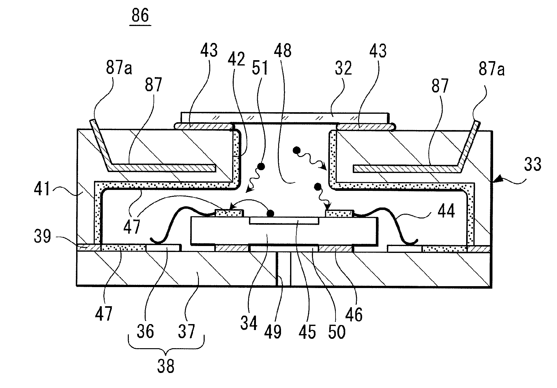
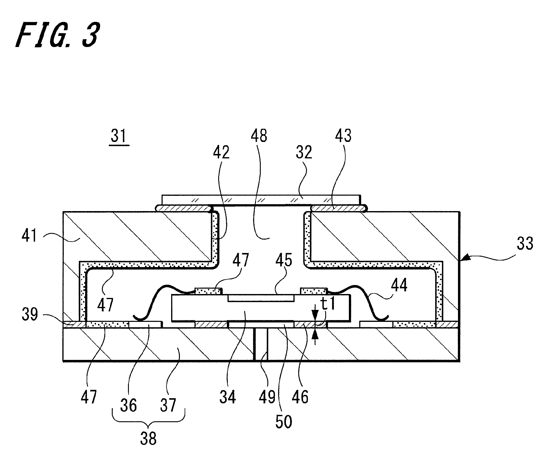
[0039]FIG. 3, FIG. 4A, and FIG. 4B illustrate an example of a package-type solid-state imaging apparatus according to an embodiment of the invention.

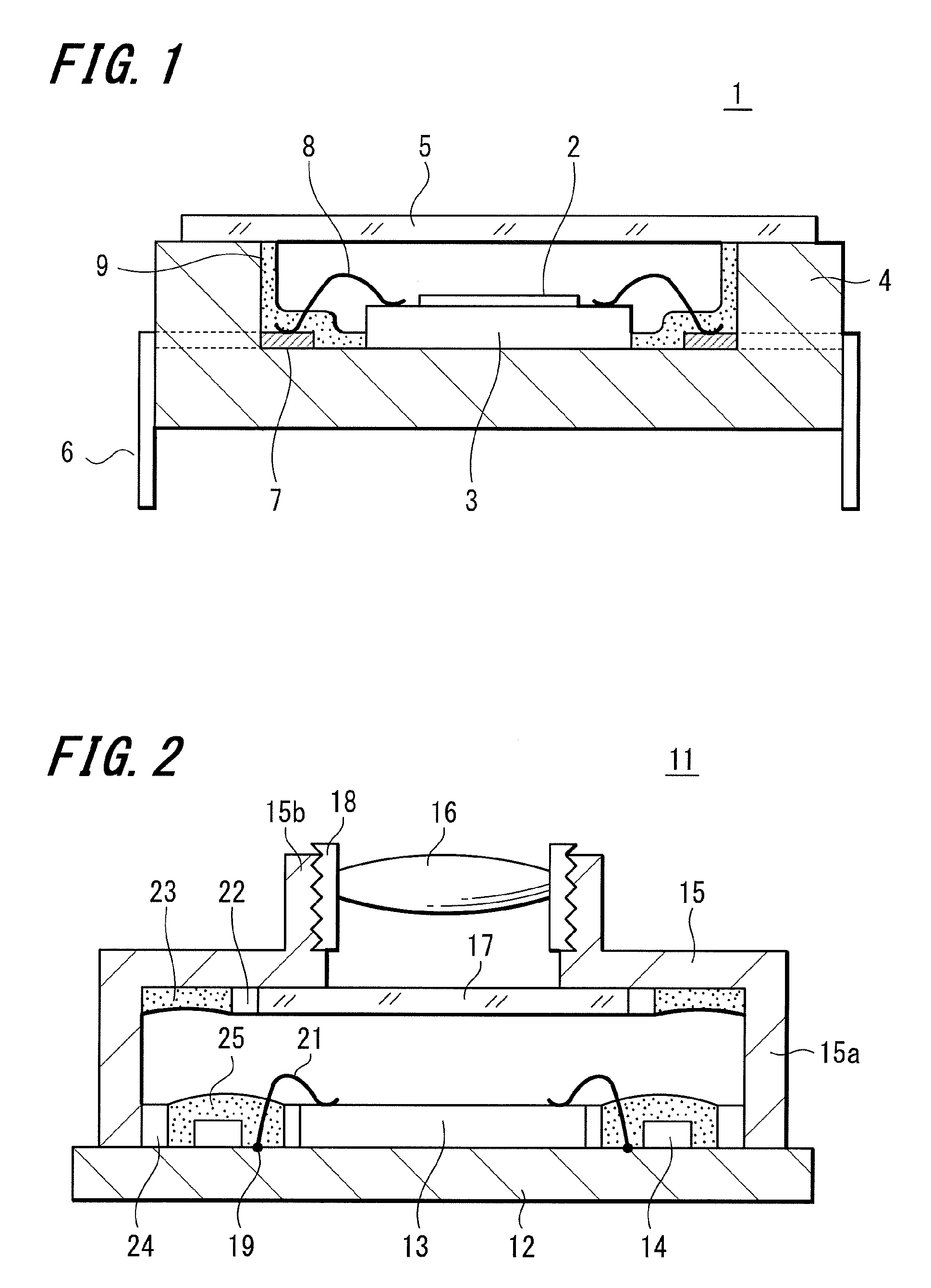
[0040]A solid-state imaging apparatus 31 according to this embodiment includes a package 33 having an optically transparent member 32, and a solid-state imaging device chip 34 such as a CCD image sensor or a CMOS image sensor enclosed in the package 33. The package 33 includes a substrate module 38, in which a circuit wiring 36 of a predetermined pattern is formed on the surface of an insulating substrate 37, and a cover body 41 connected with the substrate module 38 and protecting the solid-state imaging device chip 34. The optically transparent member 32 is connected with the cover body 41 such that an opening 42, through which an incident light enters, is closed. The substrate module 38 and the cover body 41 are hermetically connected th...


PUM


Abstract

A solid-state imaging apparatus is provided. A solid-state imaging device chip is enclosed in a package having an optically transparent member. An adhesive layer is formed on an internal surface of the package, and a penetration hole is formed in a bottom part of the package to communicate with an open space in the package.

Description

CROSS REFERENCES TO RELATED APPLICATIONS[0001]The invention contains subject matter related to Japanese Patent Application JP 2007-089256 filed in the Japanese Patent Office on Mar. 29, 2007, the entire contents of which being incorporated herein by reference.BACKGROUND OF THE INVENTION[0002]1. Field of the Invention[0003]The invention relates to a solid-state imaging apparatus, in particular to a package-type solid-state imaging apparatus enclosing a solid-state imaging device chip in a package.[0004]2. Description of the Related Art[0005]Recently, as a solid-state imaging apparatus to be mounted in an electronic device module such as a camera module used in a video camera, a digital camera, a mobile-phone with a camera, etc., a package-type solid-state imaging apparatus is widely adopted.[0006]FIG. 1 illustrates an example of a package-type solid-state imaging apparatus of related art. A package-type solid-state imaging apparatus 1 encloses in a package 4 a solid-state imaging dev...

Claims


Application Information

Patent Timeline
Patent Type & Authority Applications(United States)
IPC IPC(8): H01L31/00H01L23/02H01L27/14H04N5/335H04N5/369H04N5/372H04N5/374
CPCH01L23/26H01L27/14618H01L31/0203H01L31/0232H01L2924/09701H04N5/2251H04N5/2257H01L2224/48091H01L2224/48227H01L2224/48471H01L2224/48472H01L2224/8592H01L2924/00014H01L2924/00G03B17/02H01L2924/16195H01L31/02325B81B7/0067H04N23/52H04N23/57H01L2224/4554
Inventor YAJIMA, ATSUSHIKATAYAMA, TOKIKO
Owner SONY CORP
Why Eureka
Try Eureka