

Semiconductor Package and Method for Fabricating the Same
Inactive Publication Date: 2008-10-02
GLOBALFOUNDRIES INC
View PDF15 Cites 75 Cited by
- Summary
- Abstract
- Description
- Claims
- Application Information
AI Technical Summary
Benefits of technology
[0013]In accordance with the present invention, electric power can be supplied to the central portion of the chip through a conductor plate having small electric resistance. Therefore, compared with when connections are established only by high resistance wiring, a voltage drop at the central portion of the chip can be more reduced. In addition, the placement of a pad to be arranged
Problems solved by technology
This may cause instabil
Method used
View moreImage
Smart ImageViewing Examples

Examples
 PUM
 Abstract
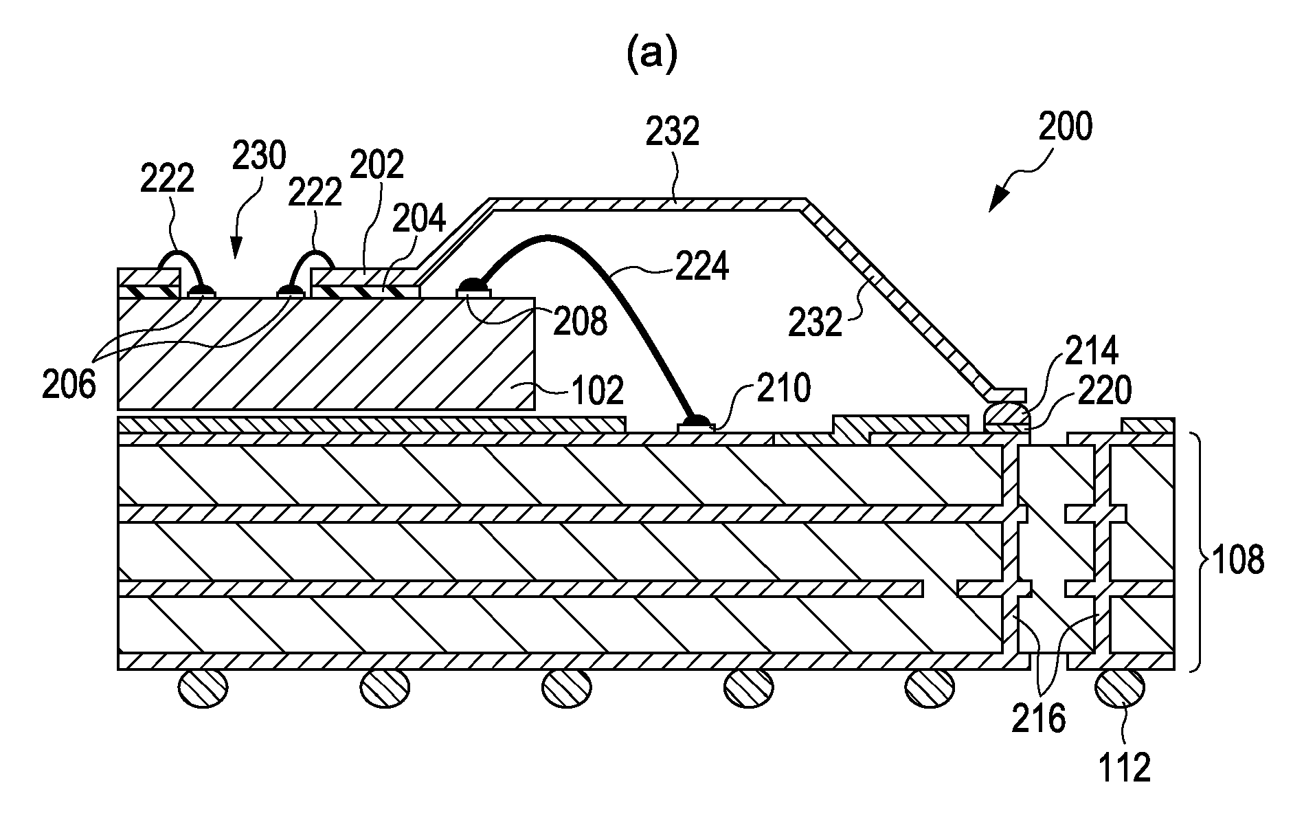
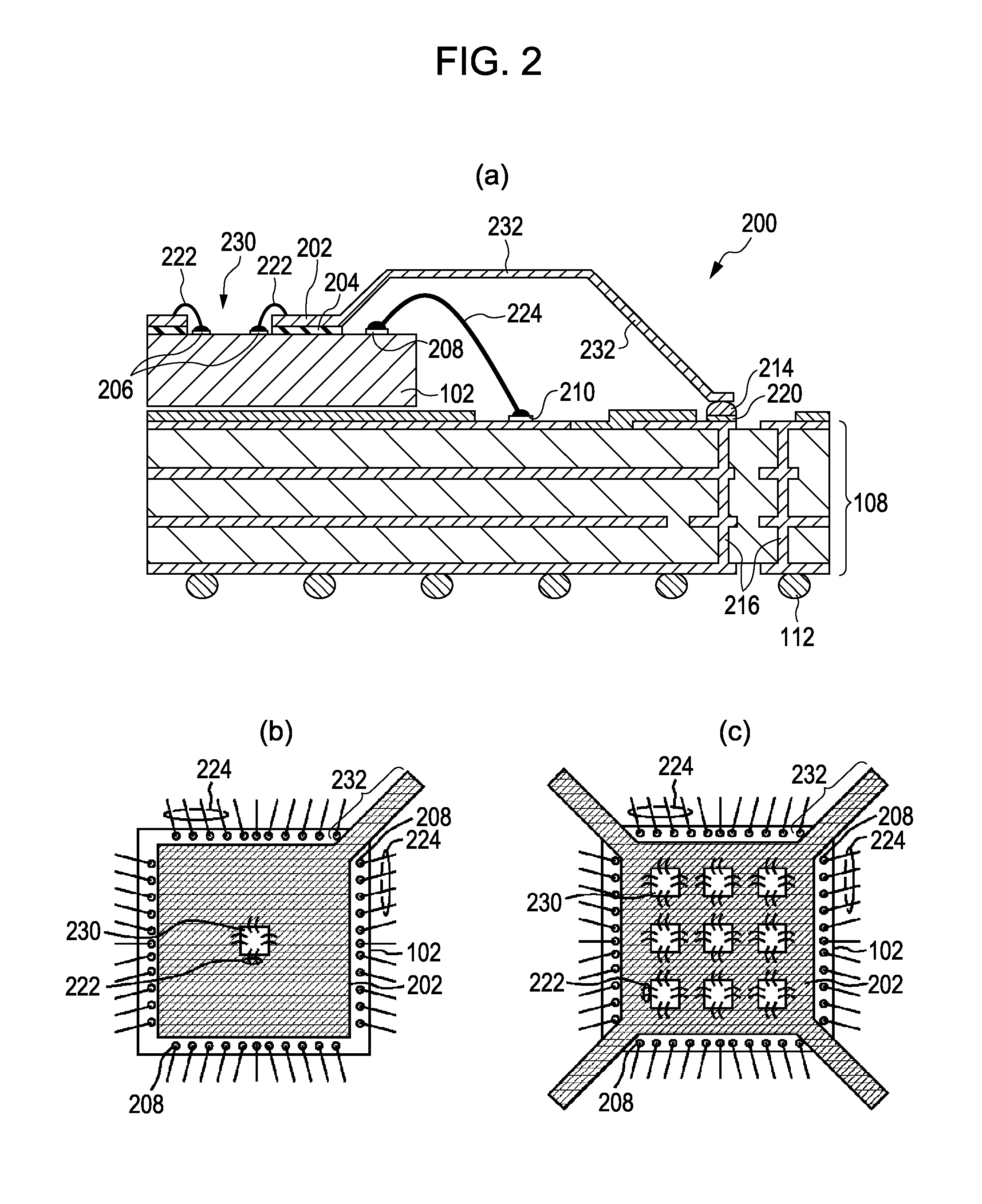
A semiconductor package includes a wiring substrate, a semiconductor chip, and a conductor plate in order to reduce a voltage drop at the central portion of a chip caused by wiring resistance from a peripheral connection pad disposed on the periphery of the chip in the semiconductor package. Central electrode pads for use in ground/power-supply are disposed on the central portion of the chip. The conductor plate for use in ground/power-supply is disposed on the chip such that an insulating layer is disposed therebetween. The central electrode pads on the chip and the conductor plate are connected together by wire bonding through an opening formed in the insulating layer and the conductor plate. An extraction portion of the conductor plate is connected to a power-supply wiring pad on the wiring substrate. The central electrode pads and the conductor plate may also be connected together using gold stud bumps. Preferably, the conductor plate is composed of a multilayer structure of two or more layers, and each conductor plate is used in power-supply wiring or ground wiring.
Description
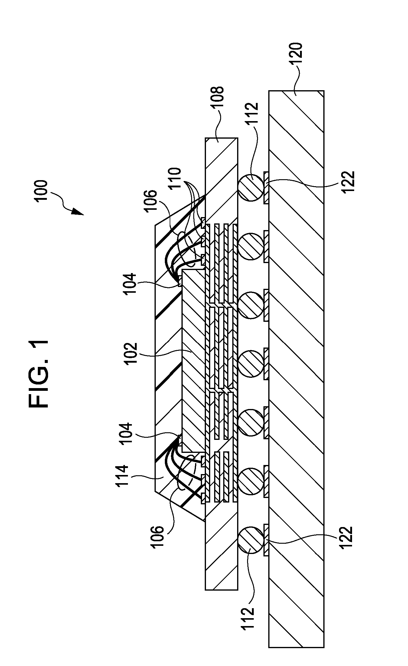
TECHNICAL FIELD[0001]The present invention relates to a semiconductor package mounted on a circuit board. In particular, the present invention relates to a semiconductor package structure for reducing a voltage drop at a central portion of a semiconductor chip in a ball grid array (BGA) package and to a method for fabricating the same.BACKGROUND ART[0002]Examples of a surface-mount package for a semiconductor chip include BGAs and quad flat packages (QFPs). A BGA is a surface-mount package developed for a large scale integrated circuit (LSI) that has more pins than those in a QFP, which is a flat package that has leads extending in four directions. BGAs are very much used, as semiconductor packages for high-speed devices, in portable machines, such as cellular phones, or personal computers. A BGA package is joined to a mounting board by use of conductive balls (bumps) arranged in an array on its back as external terminals, instead of using a lead frame. Because the entire back surfa...
Claims
Login to View More Application Information
Patent Timeline
 IPC IPC(8): H01L23/49H01L21/60
CPCH01L23/3128H01L23/49811H01L23/49822H01L23/49833H01L24/05H01L24/06H01L24/36H01L24/40H01L24/41H01L24/45H01L24/49H01L24/73H01L24/83H01L24/84H01L24/91H01L2224/0401H01L2224/04042H01L2224/05555H01L2224/05556H01L2224/05644H01L2224/06136H01L2224/32225H01L2224/45144H01L2224/48091H01L2224/48227H01L2224/48247H01L2224/48465H01L2224/49171H01L2224/73215H01L2224/73221H01L2224/73265H01L2224/83191H01L2224/838H01L2224/84203H01L2224/85191H01L2924/01004H01L2924/01005H01L2924/01028H01L2924/01029H01L2924/01046H01L2924/01047H01L2924/0105H01L2924/01074H01L2924/01077H01L2924/01078H01L2924/01079H01L2924/01082H01L2924/014H01L2924/0781H01L2924/14H01L2924/15311H01L2924/19041H01L2924/30107H01L24/29H01L24/32H01L24/48H01L2224/2919H01L2224/29298H01L2924/01006H01L2924/01033H01L2924/01045H01L2924/0665H01L2224/29101H01L2224/32245H01L2224/4826H01L2224/92247H01L2924/0132H01L2924/0001H01L2924/1517H01L2224/29111H01L2224/48644H01L2924/00013H01L24/39H01L24/34H01L2924/00014H01L2924/00H01L2924/00012H01L2924/00011H01L2224/29099H01L2224/29199H01L2224/29299H01L2224/2929H01L2224/45015H01L2924/181H01L2224/40225H01L2224/40095H01L2224/37011H01L2224/49109H01L2224/371H01L2224/84801H01L2224/37147H01L2224/3754H01L24/37H01L2224/8485
InventorHISADA, TAKASHIYONEHARA, KATSUYUKI
OwnerGLOBALFOUNDRIES INC