Manufacture of 3 dimensional MIM capacitors in the last metal level of an integrated circuit

a technology of metal insulation metal and capacitors, applied in the field of microelectronics, can solve the problems of manufacturing defects in sections of devices, capacitors generally have a limited capacity, and it is more difficult to incorporate metallic tracks and vias in the interconnection layer

Active Publication Date: 2008-10-02
STMICROELECTRONICS SRL
View PDF14 Cites 22 Cited by
  • Summary
  • Abstract
  • Description
  • Claims
  • Application Information

AI Technical Summary

Benefits of technology

[0025]The given insulating layer may have a thickness greater than 0.9 μm. The other insulating layer may have a thickness of less than 3 μm.
[0026]A micro-electronic device may be fitted with one or more 3 dimensional capacitors, and may include a substrate and a plurality of metallic interconnection levels superposed on the substrate and featuring respectively one or several horizontal metallic strips. There may be at least one given horizontal metallic strip of a given metallic interconnection level, formed in the thickness of a given insulating layer, wherein one or several trenches pass through the thickness of the given insulating layer. The trenches may be fitted respectively with walls covered by a stack formed of at least one first thin metallic layer in contact with the walls, at least one thin dielectric lay...

Problems solved by technology

The resulting size makes it more difficult to incorporate metallic tracks and vias in the interconnection layers.
These capacitors generally have a limited capacity.
These hillocks tend to cause manufacturing defects in sections of the device located above the 5th metal level and to downgrade the electrical performances of the MIM capacitor, especiall...

Method used


Image

  • Manufacture of 3 dimensional MIM capacitors in the last metal level of an integrated circuit
  • Manufacture of 3 dimensional MIM capacitors in the last metal level of an integrated circuit
  • Manufacture of 3 dimensional MIM capacitors in the last metal level of an integrated circuit

Examples


Embodiment Construction

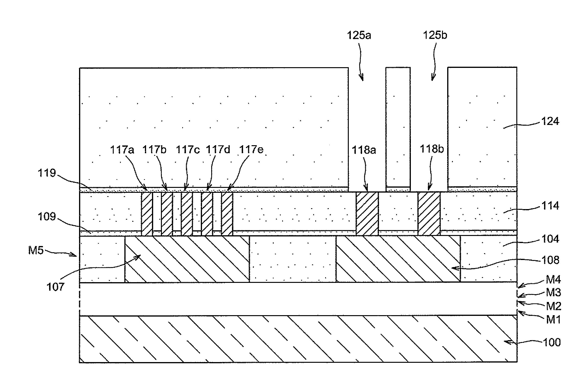
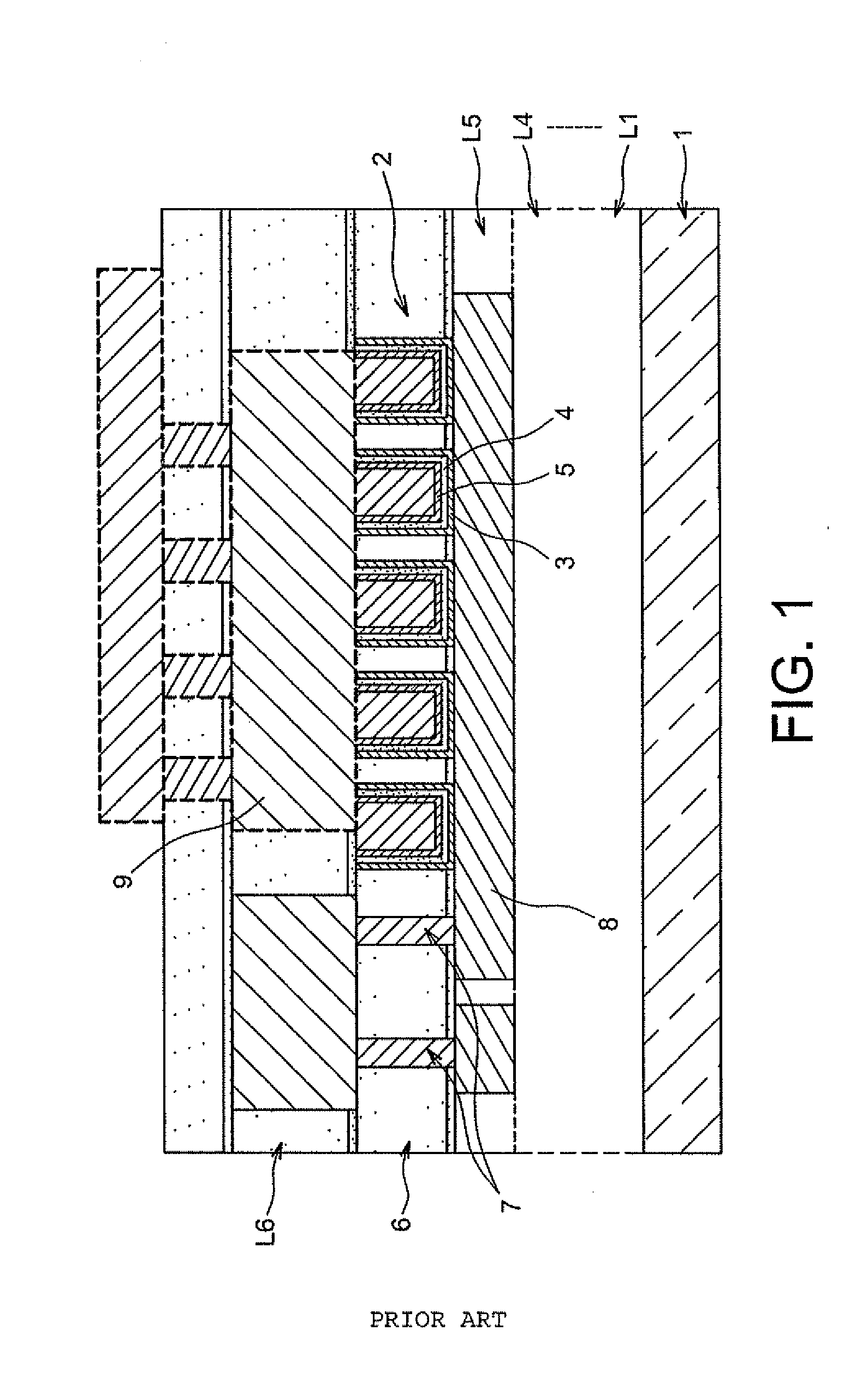
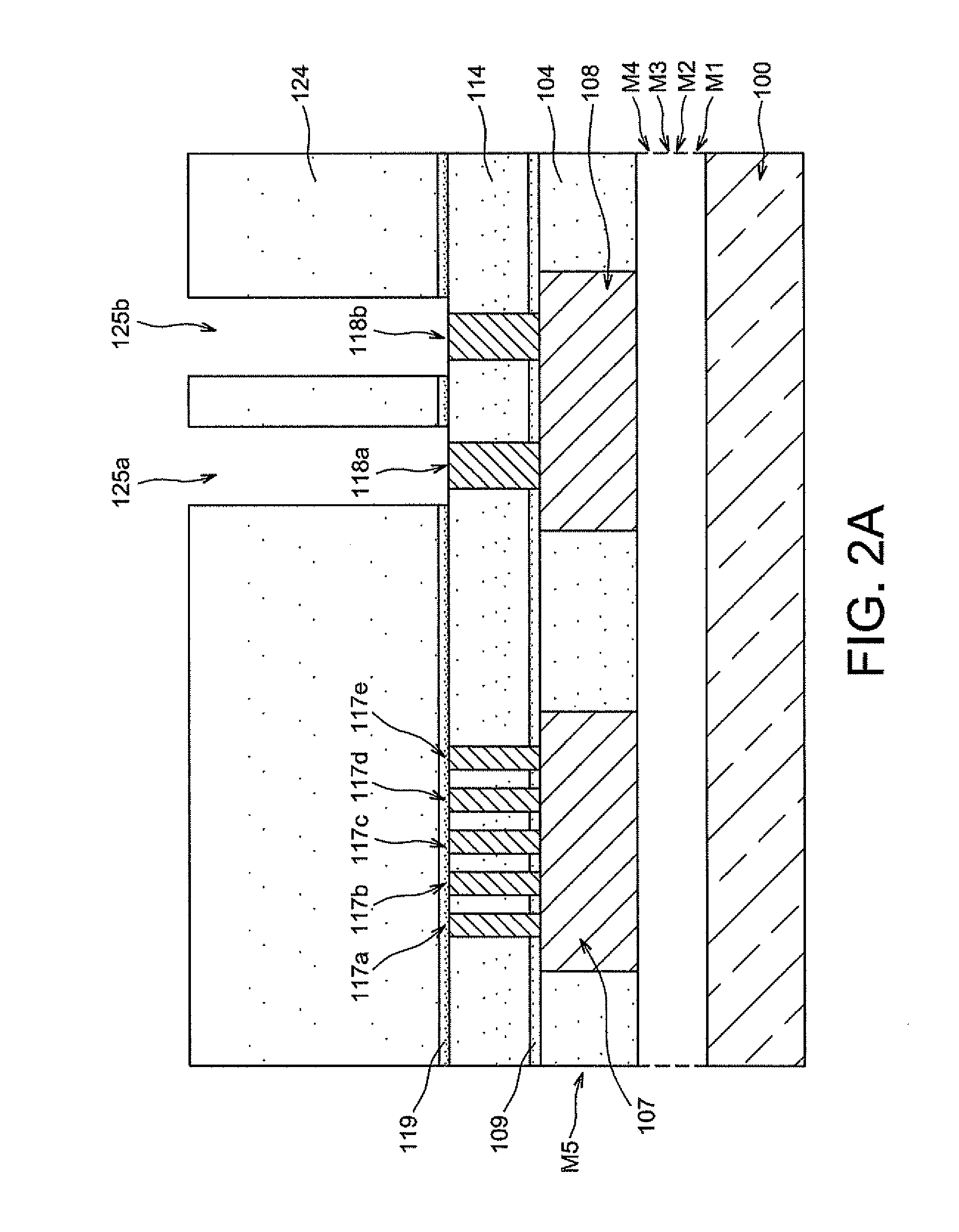
[0040]Similar or equivalent parts to those of the various figures bear the same numerical references so as to facilitate changing from one figure to another, and the various parts shown in the figures are not necessarily to a uniform scale, to make the figures easier to read.

[0041]One example of a manufacturing method of a micro-electronic device will now be provided with reference to FIGS. 2A-2D.

[0042]The initial material of this method may be an integrated circuit being manufactured, for example, a circuit comprising at least one module dedicated to radio-frequency and / or analog applications. This circuit comprises a substrate 100, on which a plurality of components have been formed and may be already fitted with a plurality of superposed metallic interconnection levels, for example five metallic interconnection levels M1, M2, M3, M4, M5 (the components and the four first metallic interconnection levels M1, . . . , M4, are represented by a block in dotted lines in FIGS. 2A-2D) eac...


PUM

PropertyMeasurementUnit
Thicknessaaaaaaaaaa
Heightaaaaaaaaaa
Metallic bondaaaaaaaaaa

Abstract

A method is for fabricating an integrated circuit formed from a substrate and including several metallic interconnection levels in which, in a same plane parallel to the main plane of the substrate, is a plurality of thick horizontal metallic interconnection lines, as well as one or several MIM capacitors fitted with metallic electrodes that are orthogonal to the main plane of the substrate.

Description

FIELD OF THE INVENTION[0001]The invention relates to the field of microelectronics and in particular, to that of 2 or 3 dimensional MIM (Metal-Insulator-Metal) capacitors in integrated circuits.[0002]It covers the manufacture of an integrated circuit formed from a substrate and comprising several metallic interconnection levels in which, in a plane parallel to the main plane of the substrate, is a plurality of thick horizontal metallic lines, as well as one or several MIM capacitors fitted with metallic electrodes, featuring portions that are orthogonal to the main plane of the substrate and portions that are parallel to the main plane of the substrate. The invention has applications in particular in the field of integrated circuits fitted with at least one RF and / or analog module.[0003]The invention provides improvements in terms of the capacity and / or density of integration of the MIM capacitors in an integrated circuit, and adapts to the integrated circuit technologies in which t...

Claims


Application Information

Patent Timeline
IPC IPC(8): H01G4/35H01G9/00B23K1/20
CPCH01L23/5223H01L23/53238Y10T428/12986Y10T29/417H01L28/91H01L2924/0002H01L2924/00
Inventor CREMER, SEBASTIENGIRAUDIN, JEAN-CHRISTOPHESERRET, EMMANUELLE
Owner STMICROELECTRONICS SRL
Why Eureka
Try Eureka