Perovskite thin-film photovoltaic cell and manufacturing method thereof
A thin-film photovoltaic cell, perovskite technology, applied in photovoltaic power generation, circuits, electrical components, etc., can solve the problems of acid and alkali resistance of the ZnO electron transport layer, long-term stability of the battery, and electron-hole recombination. Conducive to the promotion of technology, reducing production costs, and the effect of simple production processes
- Summary
- Abstract
- Description
- Claims
- Application Information
AI Technical Summary
Problems solved by technology
Method used
Image
Examples
Embodiment 1
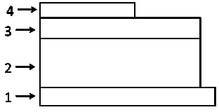
[0032] 1) Wash. In the test, the FTO conductive glass substrate should be cleaned and dried first. First, cut the conductive glass to the required size with a glass knife, clean it with a detergent, and then rinse it with deionized water. Then place it in an ultrasonic cleaner to clean it with acetone, ethanol, and ionized water in sequence, and finally dry it with nitrogen to obtain a substrate with a clean surface required for the experiment.
[0033] 2) Perovskite solution configuration. CH 3 NH 3I and PbCl 2 Dissolve in dimethylformamide at a molar ratio of 3:1, stir at room temperature for 24 hours and set aside;
[0034] 3) Preparation of perovskite light-absorbing layer. Spin-coat a layer of 2 micron thick CH on the FTO with controlled spinner speed 3 NH 3 PB 3-x Cl x The perovskite light-absorbing layer was then annealed at 100 degrees Celsius for forty-five minutes.
[0035] 4) Preparation of hole transport layer. On the thin film covered with perovskite l...
Embodiment 2
[0039] 1) Wash. With embodiment 1.
[0040] 2) Perovskite solution configuration. With embodiment 1.
[0041] 3) Preparation of perovskite light-absorbing layer. Spin-coat a layer of perovskite light-absorbing layer with a thickness of 1.5 μm on the FTO with a spinner, and then anneal at 100 °C for forty-five minutes.
[0042] 4) Preparation of hole transport layer. With embodiment 1.
[0043] 5) Electrode preparation. With embodiment 1.
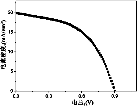
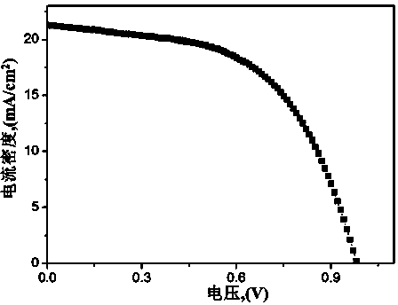
[0044] 6) Test. At AM1.5, the effective area of the active layer is 0.09 cm 2 The battery is tested under the conditions. The obtained photoelectric conversion efficiency parameters are, open circuit voltage 0.99 V, short circuit current density 21.33 mA / cm 2 , fill factor 0.55, conversion efficiency 11.55%.
Embodiment 3
[0046] 1) Wash. With embodiment 1.
[0047] 2) Perovskite solution configuration. With embodiment 1.
[0048] 3) Preparation of perovskite light-absorbing layer. A perovskite light-absorbing layer with a thickness of 1 μm was spin-coated on the FTO with a spinner, and then annealed at 100 °C for forty-five minutes.
[0049] 4) Preparation of hole transport layer. With embodiment 1.
[0050] 5) Electrode preparation. With embodiment 1.
[0051] 6) Test. At AM1.5, the effective area of the active layer is 0.09 cm 2 The battery is tested under the conditions. The obtained photoelectric conversion efficiency parameters are, open circuit voltage 1.04 V, short circuit current density 21.35 mA / cm 2 , fill factor 0.61, conversion efficiency 13.44%.
PUM
 Abstract
Description
Claims
Application Information


