Method and system for patterning a mask layer

a mask layer and mask technology, applied in the field of mask layer patterning, can solve the problems of increasing run time and process errors, limiting layer-to-layer accuracy, and causing various difficulties

Active Publication Date: 2008-10-02
XEROX CORP
View PDF21 Cites 15 Cited by
  • Summary
  • Abstract
  • Description
  • Claims
  • Application Information

AI Technical Summary

Problems solved by technology

However, in using methods such as that shown in FIGS. 1(a)-1(c), various difficulties arise.
This limits the layer-to-layer accuracy and, for cases where the run-out is very large or non-uniform, the printed circuit board 10 typically needs to be scraped.
In addition, using multiple masks 16 increases run time and process errors.
However, these systems require that extra steps be taken in the process to remove the wax, which can be difficult.

Method used


Image

  • Method and system for patterning a mask layer
  • Method and system for patterning a mask layer
  • Method and system for patterning a mask layer

Examples


Embodiment Construction

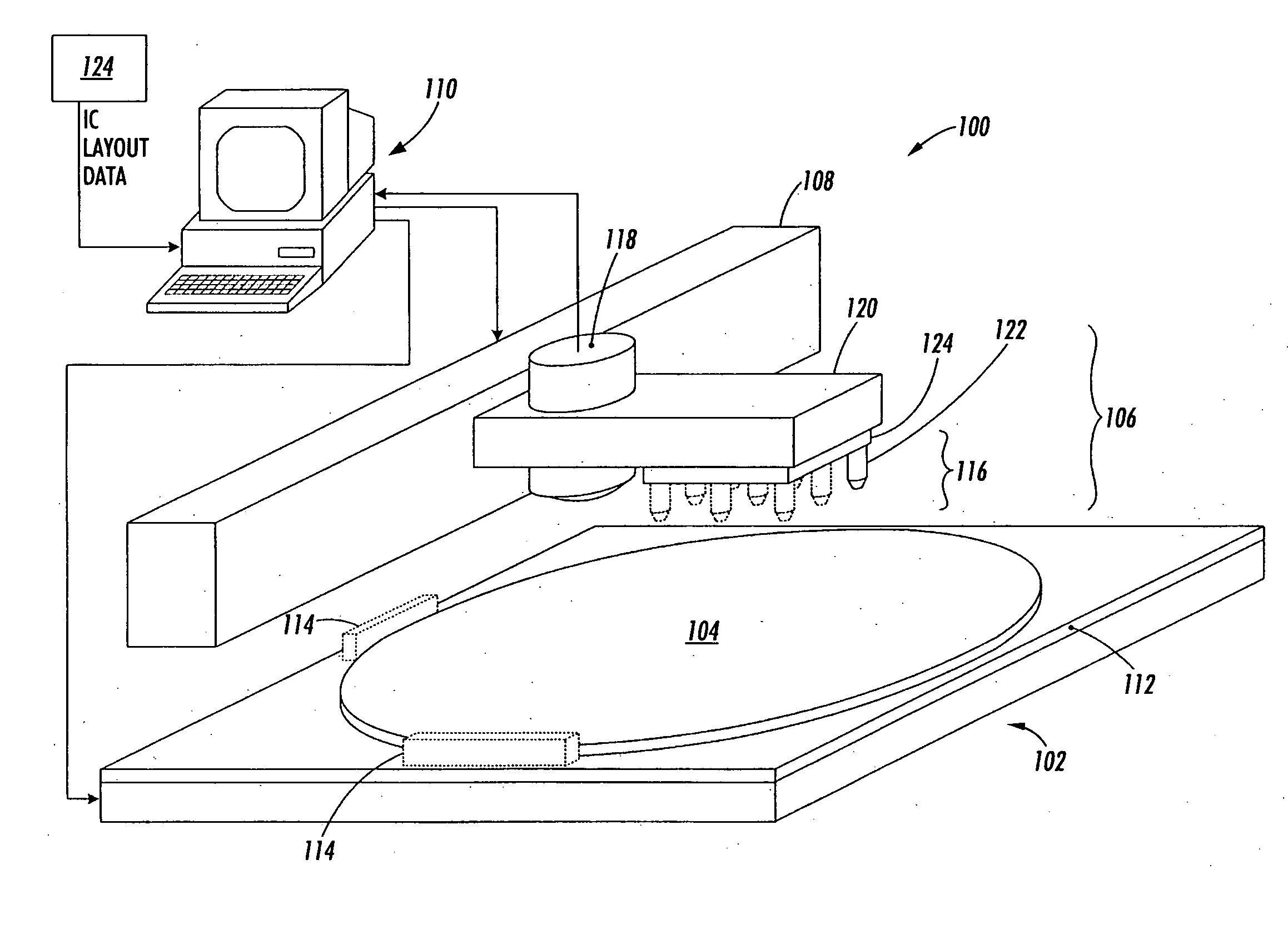
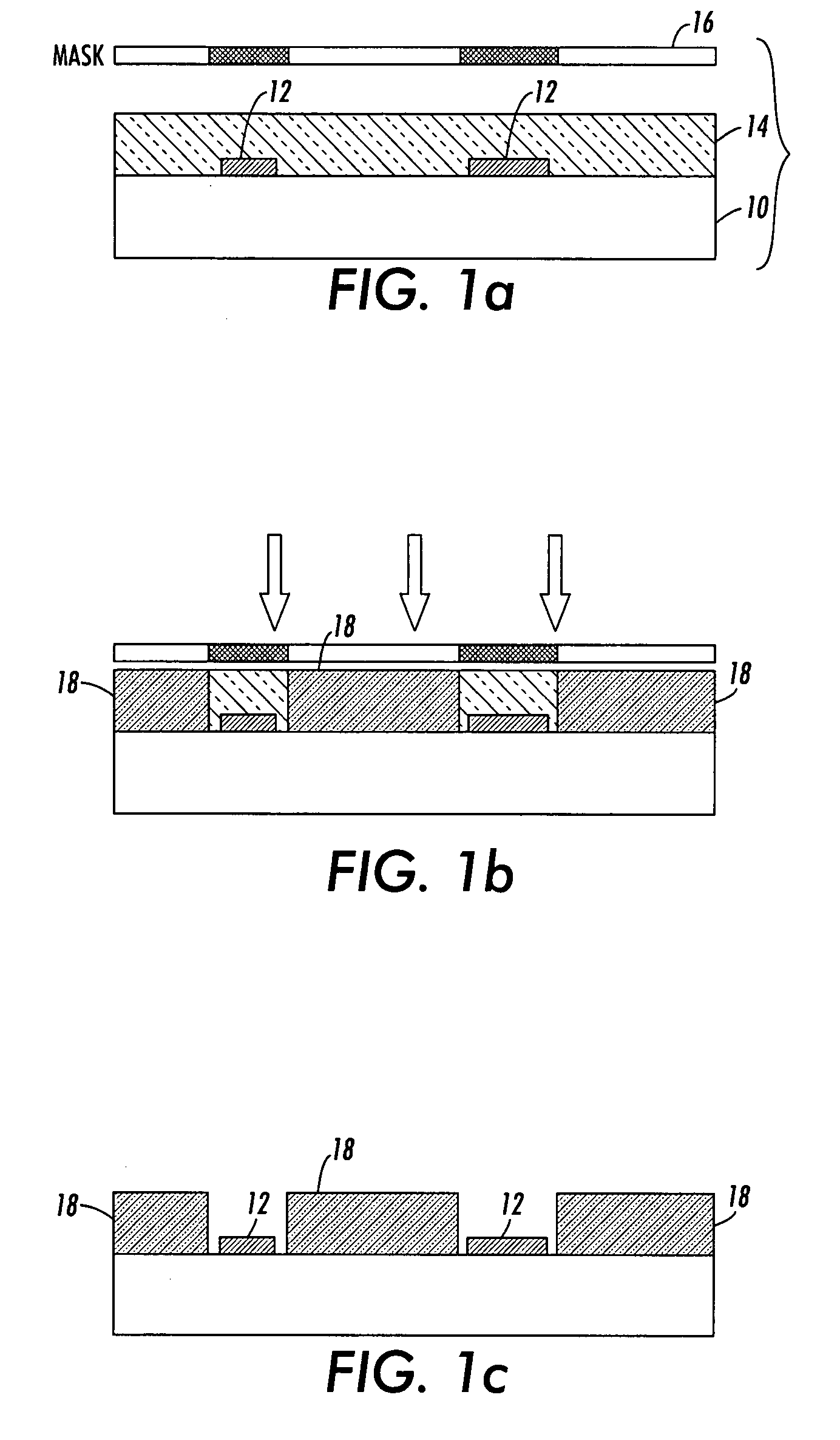
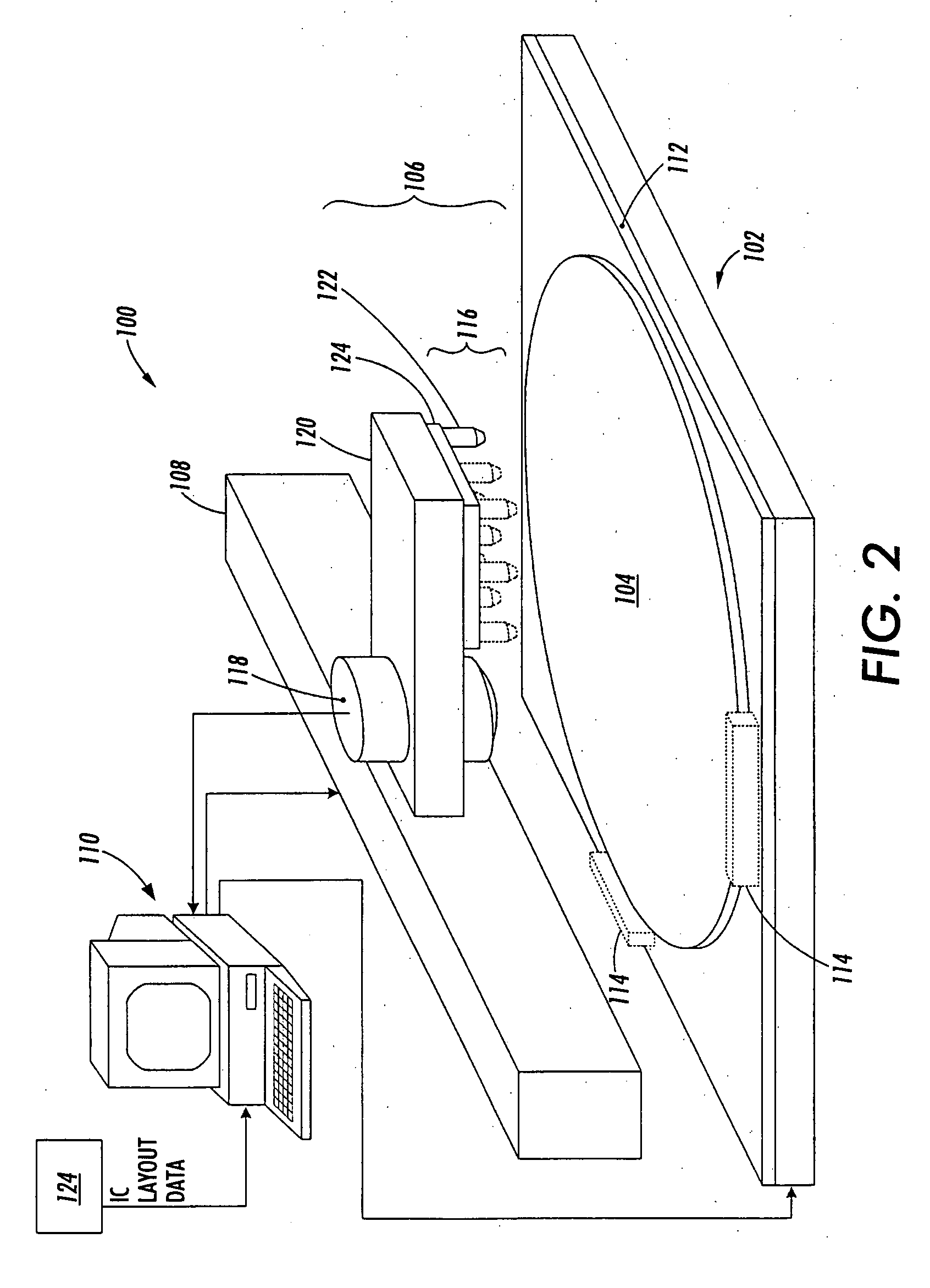
[0030]The presently described embodiments use a printing process, e.g. a wax printing technique, to pattern a mask layer (such as a soldermask layer) of, for example, a printed circuit. Substantially all other conventional processes in developing soldermask and exposure processes can be maintained. According to the presently described embodiments, each printed circuit, e.g. a printed circuit board (PCB), will have a unique pattern that matches uniform and non-uniform runout. The pattern, in one form, is comprised of single drops of wax having a specified gap therebetween to make the process transparent to the current industry practice. Furthermore, the single drops can be used for both large and small areas without any development time differences. In at least one form, the wax pattern and the soldermask in the gap are removed during development.

[0031]One advantage is that large areas and small areas can be patterned without loading effect and can be patterned evenly, due to uniform...


PUM

PropertyMeasurementUnit
transparentaaaaaaaaaa
areasaaaaaaaaaa
homogenousaaaaaaaaaa

Abstract

The presently described embodiments use a printing process, e.g. a wax printing technique, to pattern a mask layer (such as a soldermask layer) of, for example, a printed circuit. Substantially all other conventional processes in developing soldermask and exposure processes can be maintained. According to the presently described embodiments, each printed circuit will have a unique pattern that matches uniform and non-uniform runout. In one form, the pattern is comprised of wax single drops having a specified gap to make the process transparent to the current industry practice. Furthermore, the single drops can be used for both large and small areas without any development time differences. In at least one form, the wax pattern and the soldermask in the gap are removed during development.

Description

CROSS REFERENCE TO RELATED PATENTS AND APPLICATIONS[0001]This application is related to U.S. Pat. No. 6,872,320, issued Mar. 29, 2005, entitled “Method for Printing Etch Masks Using Phase Change Materials,” which is incorporated herein by reference.BACKGROUND[0002]The final lithography step in printed circuit manufacturing is mask patterning. Although a variety of ultraviolet curable materials could be used, a negative photoactive soldermask material is typically patterned using an ultraviolet (UV) source and a hard mask. With reference FIG. 1(a), a printed circuit, such as a printed circuit board 10, with a copper pattern 12 and a soldermask layer 14 disposed thereon is shown. Runout is measured. In addition, an appropriate pattern mask 16 is selected and positioned for a patterning operation.[0003]Typically, the soldermask layer is coated, or otherwise formed, on the printed circuit board 10 and the combination is then soft baked. The mask 16 is then applied. As shown in FIG. 1(b)...

Claims


Application Information

Patent Timeline
Patent Type & Authority Applications(United States)
IPC IPC(8): G03F1/00
CPCG03F7/2018H05K3/0023H05K2203/0551H05K3/28H05K3/0082
Inventor LIMB, SCOTT JONG HOSHRADER, ERIC J.SRINIVASAN, UMA
Owner XEROX CORP
Why Eureka
Try Eureka