

Shift register and level controller
- Summary
- Abstract
- Description
- Claims
- Application Information
AI Technical Summary
Benefits of technology
Problems solved by technology
Method used
Image

Examples
embodiment one
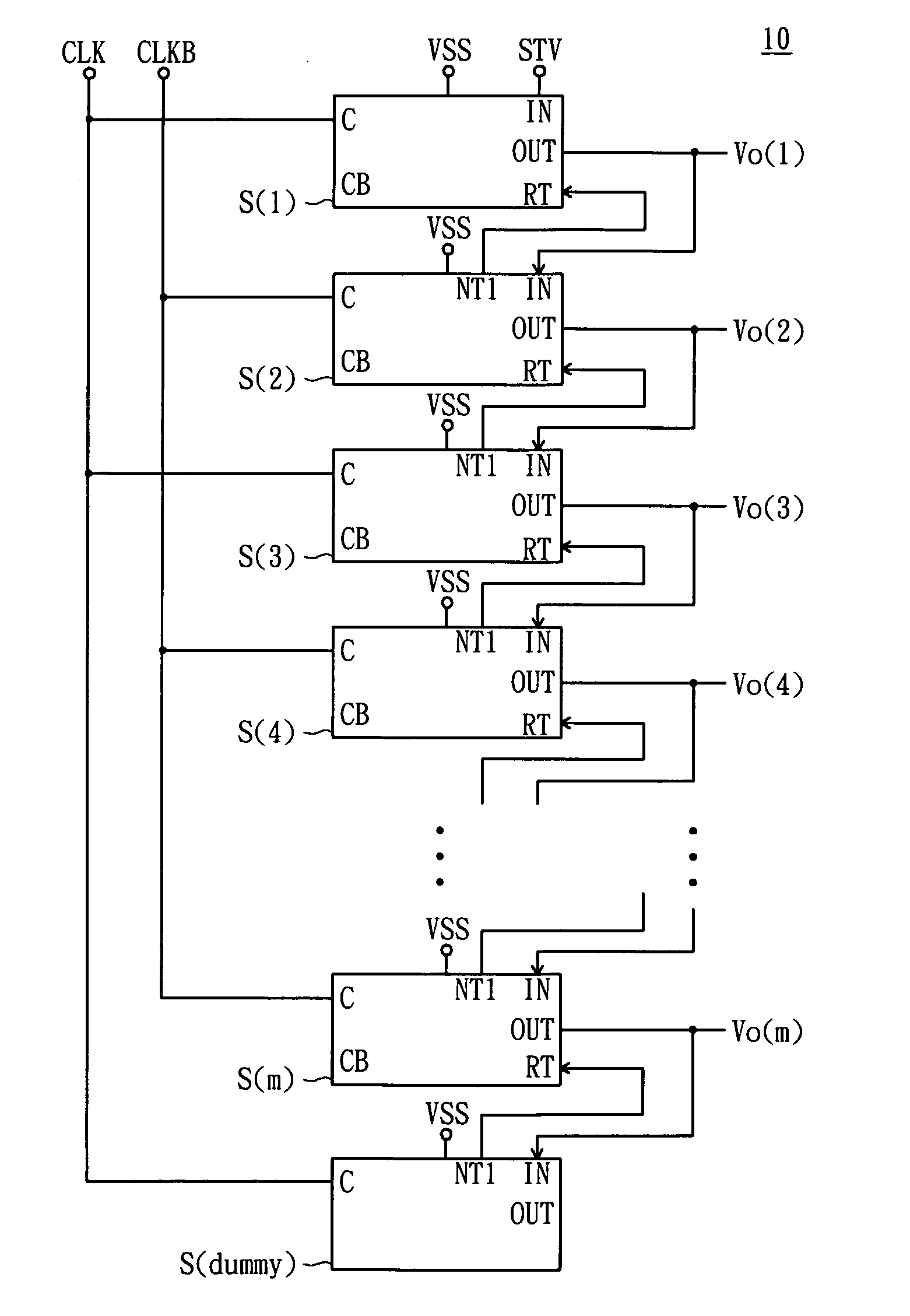
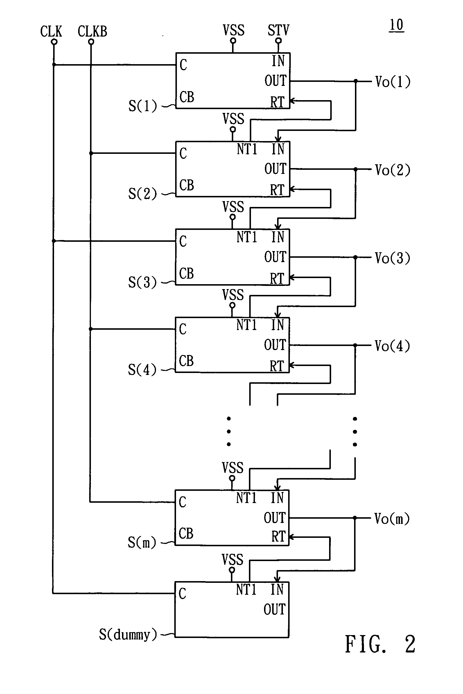
[0045]Referring to FIG. 2, a block diagram of a shift register according to a first embodiment of the invention is shown. A shift register 10 includes m shift register units S(1)-S(m) coupled in series to each other and having the same structure for instance. In the embodiment, each of the shift register units S(1)-S(m) includes an input terminal IN, an output terminal OUT, a control terminal RT, a node NT1, and a timing terminal C. The input terminal IN of the shift register unit S(1) receives a start signal STV and the input terminals IN of the shift register units S(2)-S(m) sequentially receive the scan signals Vo(1)-Vo(m−1) outputted by the output terminal of the previous stage of shift register units S(1)-S(m−1), respectively.
[0046]In the shift register units S(1)-S(m), the timing signals received by any two adjacent timing terminals C have staggered enabling time In the embodiment, the timing terminal C of the odd-stage ones in the shift register units S(1)-S(m) are exemplifie...
embodiment two
[0063]Referring to FIG. 6, a block diagram of a shift register according to a second embodiment of the invention is shown. The difference between the shift register 20 of the embodiment and the shift register 10 of the first embodiment is that each of the shift register units S′(1)-S′(m) further includes a time terminal CB for receiving an inverse clock signal compared to the clock signal received by the corresponding time terminal C.
[0064]In the shift register units S′(1)-S′(m), the timing signals received by any two adjacent timing terminals C have staggered enabling time, the timing signals received by any two adjacent timing terminals CB have staggered enabling time. The timing signals received respectively by the timing terminal CB of the n-th stage of shift register unit S′(n) and the timing terminal C of the (n+1)-th stage of shift register unit S′(n+1) have also staggered enabling time, wherein n is a natural number. In the following description, the n-th stage of shift regi...
example two
[0067]Referring to FIG. 8, a detailed circuit diagram of the shift register unit in FIG. 6 according to a second example of the second embodiment is shown. The difference between the shift register unit S2′(n) of the example and the shift register unit S1(n) is that the level lowering unit 208 of the example further includes a transistor T10, and the transistor T10 has a gate for receiving the timing signal CLKB, a drain coupled to the output terminal OUT and a source for receiving the voltage VSS. In the time periods TP1 and TP3, the transistor T10 is turned on such that the scan signal Vo(n) is equal to the voltage VSS. Therefore, the level lowering unit 208 of the example can lower down the level of the scan signal Vo(n) via the transistor T10 in the periods TP1 and TP3 to ensure that the scan signal Vo(n) maintains at the low level in the periods TP1 and TP2 and prevent the scan signal Vo(n) from increasing to a high level due to influence of circuit noise. Consequently, in addi...
PUM
 Abstract
Description
Claims
Application Information