Structure for Electrostatic Discharge in Embedded Wafer Level Packages

a technology of electrostatic discharge and embedded wafers, which is applied in the direction of semiconductor devices, semiconductor/solid-state device details, electrical apparatuses, etc., can solve the problems of damage to semiconductor chips or even their destruction

Active Publication Date: 2008-10-30
TAHOE RES LTD
View PDF10 Cites 100 Cited by
  • Summary
  • Abstract
  • Description
  • Claims
  • Application Information

AI Technical Summary

Problems solved by technology

In the case of such a method, electrostatic discharges (ESD) may occur, a

Method used


Image

  • Structure for Electrostatic Discharge in Embedded Wafer Level Packages
  • Structure for Electrostatic Discharge in Embedded Wafer Level Packages
  • Structure for Electrostatic Discharge in Embedded Wafer Level Packages

Examples


Embodiment Construction

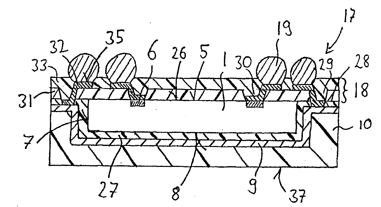
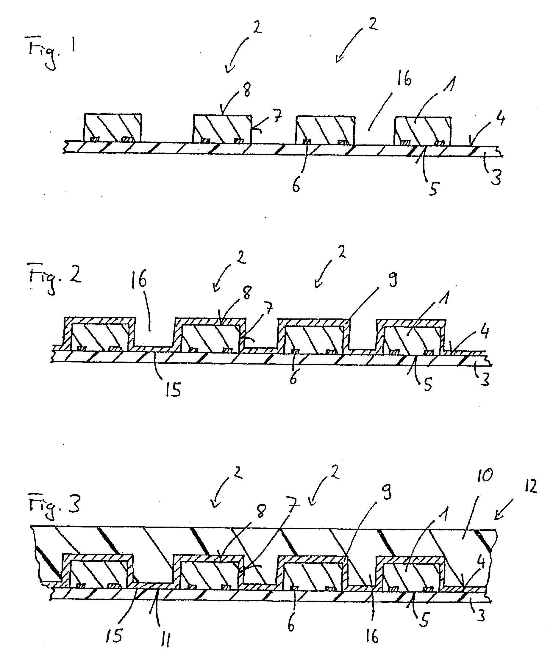
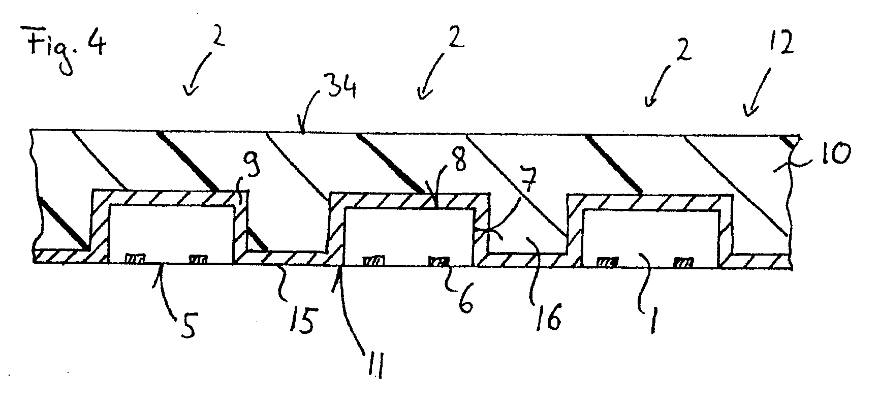
[0021]The same parts are provided with the same designations in all the figures.

[0022]FIG. 1 shows a carrier sheet 3, on the upper side 4 of which semiconductor chips 1 have been applied in semiconductor device positions 2 that are arranged in rows and columns to produce a workpiece, which in this embodiment is a panel. In this context, “workpiece” is understood as meaning an article that is still intended for further processing, for example an intermediate product in the production of semiconductor devices, such as a panel. The semiconductor chips 1 have previously been singulated from a semiconductor wafer. Interspaces 16 are formed between the semiconductor chips 1.

[0023]In this exemplary embodiment, the semiconductor chips 1 have first main surfaces 5 with active semiconductor chip structures such as integrated circuits and contact areas 6. The side faces 7 and the second main surfaces 8 of the semiconductor chips 1 are passive. Alternatively, active regions may also be arranged...


PUM


Abstract

A workpiece has at least two semiconductor chips, each semiconductor chip having a first main surface, which is at least partially exposed, and a second main surface. The workpiece also comprises an electrically conducting layer, arranged on the at least two semiconductor chips, the electrically conducting layer being arranged at least on regions of the second main surface, and a molding compound, arranged on the electrically conducting layer.

Description

BACKGROUND OF THE INVENTION[0001]The invention relates to a workpiece with semiconductor chips, such as for example a panel with semiconductor chips arranged in semiconductor device positions. It also relates to a semiconductor device and to a method for producing the workpiece.[0002]In the production of semiconductor devices, successful results have been obtained with methods in which a composite panel or so-called “reconfigured wafer” is first produced by the “wafer molding” process from semiconductor chips that are embedded with a main surface and side faces in a plastic molding compound. First main surfaces of the semiconductor chips thereby form a coplanar surface with the upper side of the plastic compound or the first main surface of the composite panel or of the “reconfigured wafer”. A wiring structure is then applied to this coplanar surface, it being possible for the plastic surface around the front side of each semiconductor chip to be used for accommodating additional te...

Claims


Application Information

Patent Timeline
IPC IPC(8): H01L23/52H01L21/4763H01L23/552
CPCH01L21/561H01L2224/0401H01L23/3128H01L23/5389H01L23/552H01L23/60H01L24/19H01L24/96H01L24/97H01L2224/04105H01L2224/20H01L2224/97H01L2924/01015H01L2924/14H01L2924/15311H01L2924/1617H01L2924/19043H01L2924/3025H01L21/568H01L2224/12105H01L23/48H01L21/565H01L2924/01006H01L2924/01033H01L2224/82H01L2924/181H01L2924/12042H01L2924/00H01L21/4853H01L21/486H01L25/50
Inventor BRUNNBAUER, MARKUSMEYER, THORSTENBRADL, STEPHANPLIENINGER, RALF
Owner TAHOE RES LTD
Why Eureka
Try Eureka