Liquid crystal display device

Inactive Publication Date: 2008-10-30
FUJITSU LTD
View PDF14 Cites 2 Cited by
  • Summary
  • Abstract
  • Description
  • Claims
  • Application Information

AI Technical Summary

Benefits of technology

[0014]In the liquid crystal display device of the aspect, since, in general, the linear expansion coefficient of liquid crystal is greater than the linear expansion coefficient of a sealing member, by making the thickness of the sealing member two times thicker than the thickness of the liquid crystal material, the difference between the volume change in the liquid crystal material due to a temperature change and the volume change in the space in which liquid crystal is sealed is made smaller so that the occurrence of defects due to the volume difference is restrained.
[0015]Since the thickness of the sealing member is made two times, more preferably, three times, thicker than the thickness of the liquid crystal material, a difference between a volume change in liquid crystal and a volume change in a space in which liquid crystal is sealed, due to a temperature change, can be made smaller so that it becomes possible to provide a liquid crystal display device that causes no defects even in a wide temperature range.

Problems solved by technology

That of a reflecting type is unstable in its reflected light quantity depending on environmental conditions, and poor in visibility; therefore, in particular, as a display device for a personal computer or the like on which a multicolor or full color displaying process is performed, a transmitting type color liquid crystal display device using color filters has been generally used.
Although these TFT-drive liquid crystal display devices have a high display quality, the light transmittance of the liquid crystal panel is in a low level of about several percents at present; consequently, a high luminance backlight is required to obtain high screen luminance.
For this reason, the power consumption by the backlight becomes greater.
Moreover, since a color displaying process is performed by using color filters, one pixel needs to be configured by three sub-pixels, and consequently, it becomes difficult to form a high-precision device and the display color purity is not sufficient.
The ferroelectric liquid crystal having spontaneous polarization has a problem in that the alignment thereof is easily deformed by an external force and is hardly recovered.
In the case when a sealing member is placed in the liquid crystal panel, a problem arises in which due to a difference in linear expansion coefficients between the liquid crystal material and the sealing member, the change in the panel volume fails to follow the change in the volume of the liquid crystal material (in particular, contraction) to cause a disturbance in the liquid crystal alignment, resulting in defects in the liquid crystal layer.
In particular, these alignment defects tend to occur near the peripheral sealed portion.
Since the alignment defects are caused by the fact that the linear expansion coefficient of the sealing member is smaller than the linear expansion coefficient of the liquid crystal material, an attempt has been made conventionally so as to make the physical properties (in particular, linear expansion coefficient) of the sealing member coincident with the physical properties of the liquid crystal material; however, this attempt has not achieved sufficient effects.
Here, the occurrence of defects due to the difference between the volume change in the liquid crystal and the volume change in the space in which the liquid crystal is sealed is a problem that might commonly occur not only in the ferroelectric liquid crystal, but also in antiferroelectric liquid crystal having spontaneous polarization as well as in a liquid crystal material having no spontaneous polarization, for example, nematic liquid crystal.
Here, in comparison with a liquid crystal material having no spontaneous polarization, the liquid crystal material having spontaneous polarization is more easily susceptible to defects to cause a more serious problem.

Method used


Image

  • Liquid crystal display device
  • Liquid crystal display device
  • Liquid crystal display device

Examples


embodiment 1

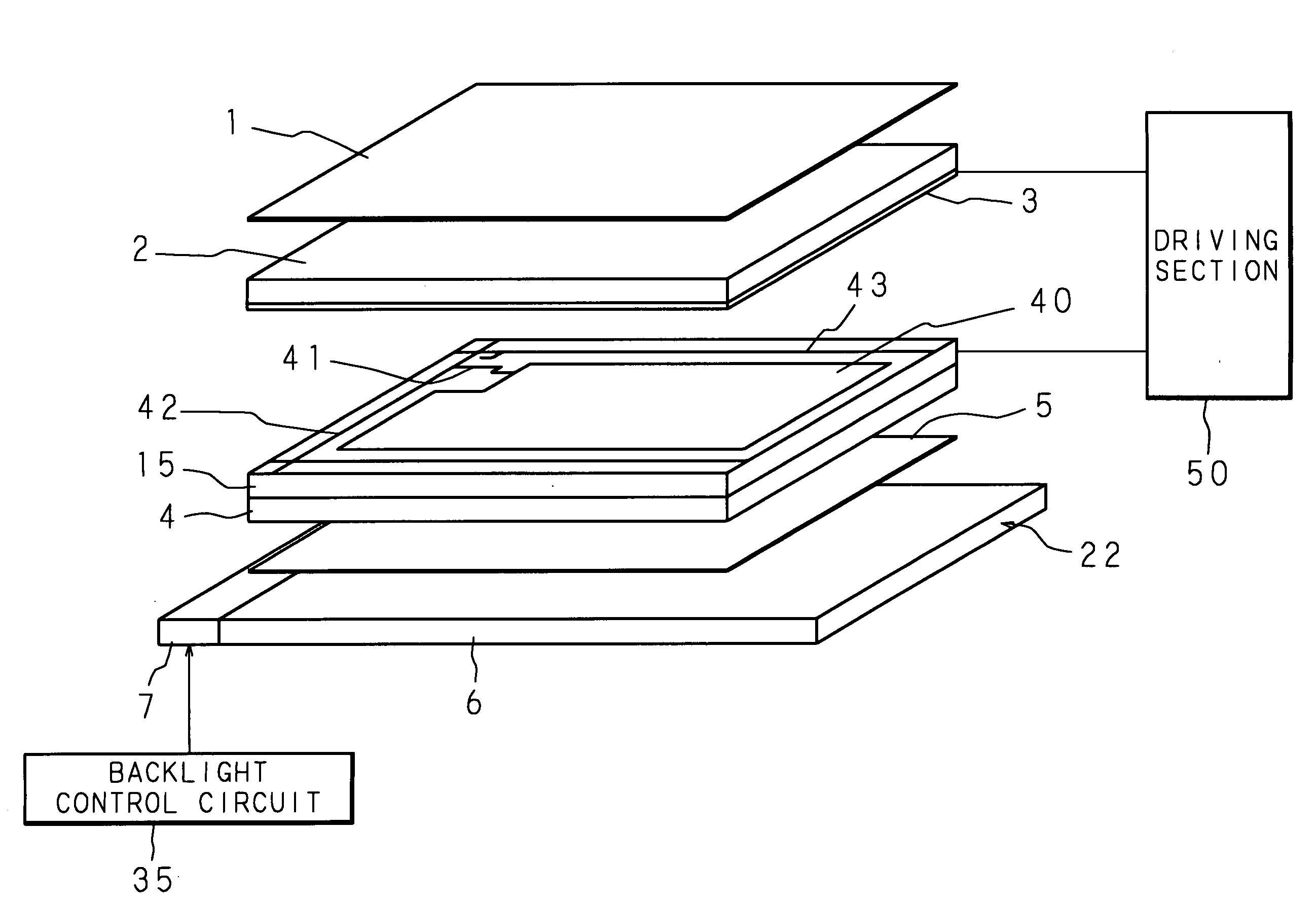
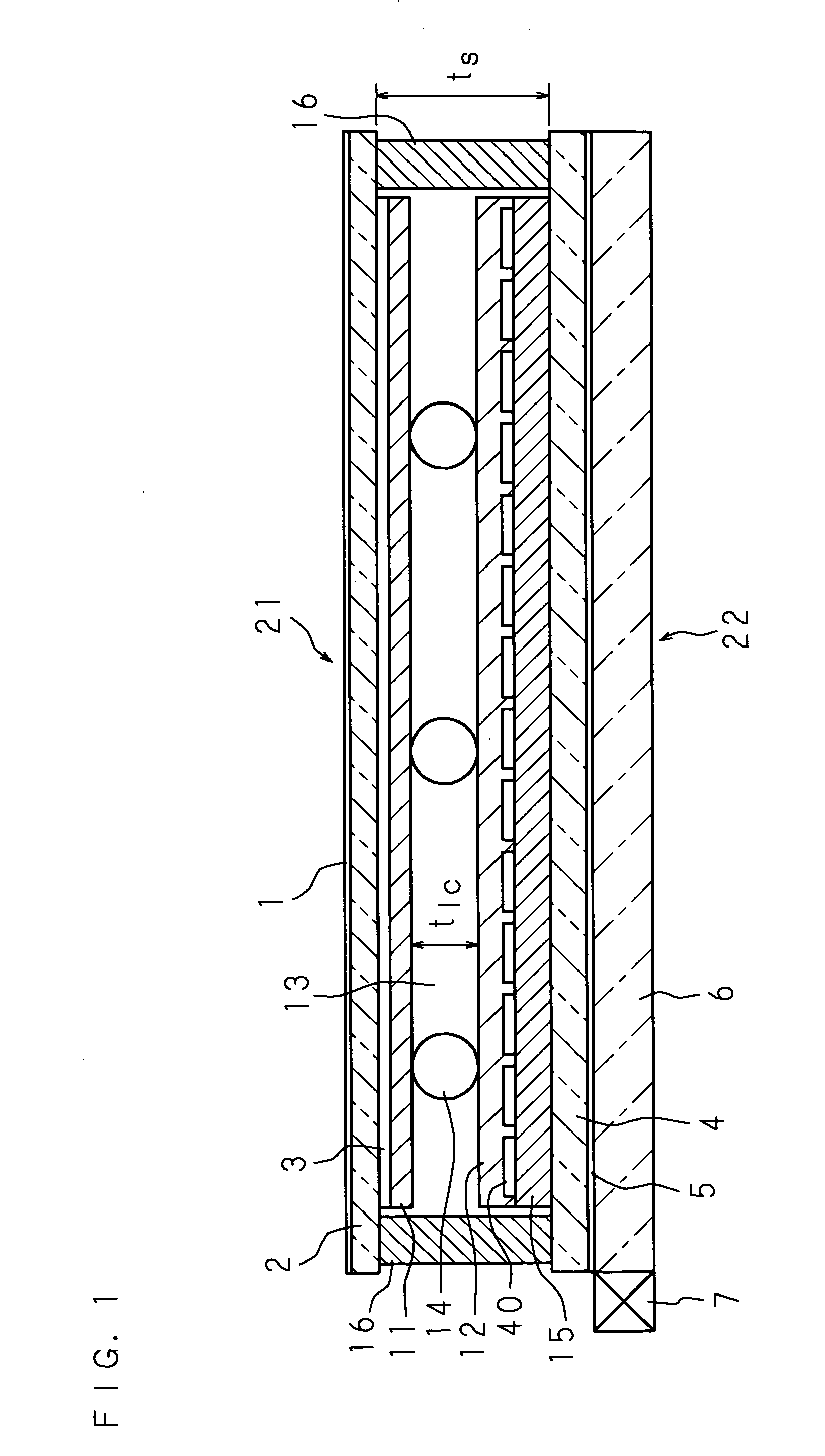
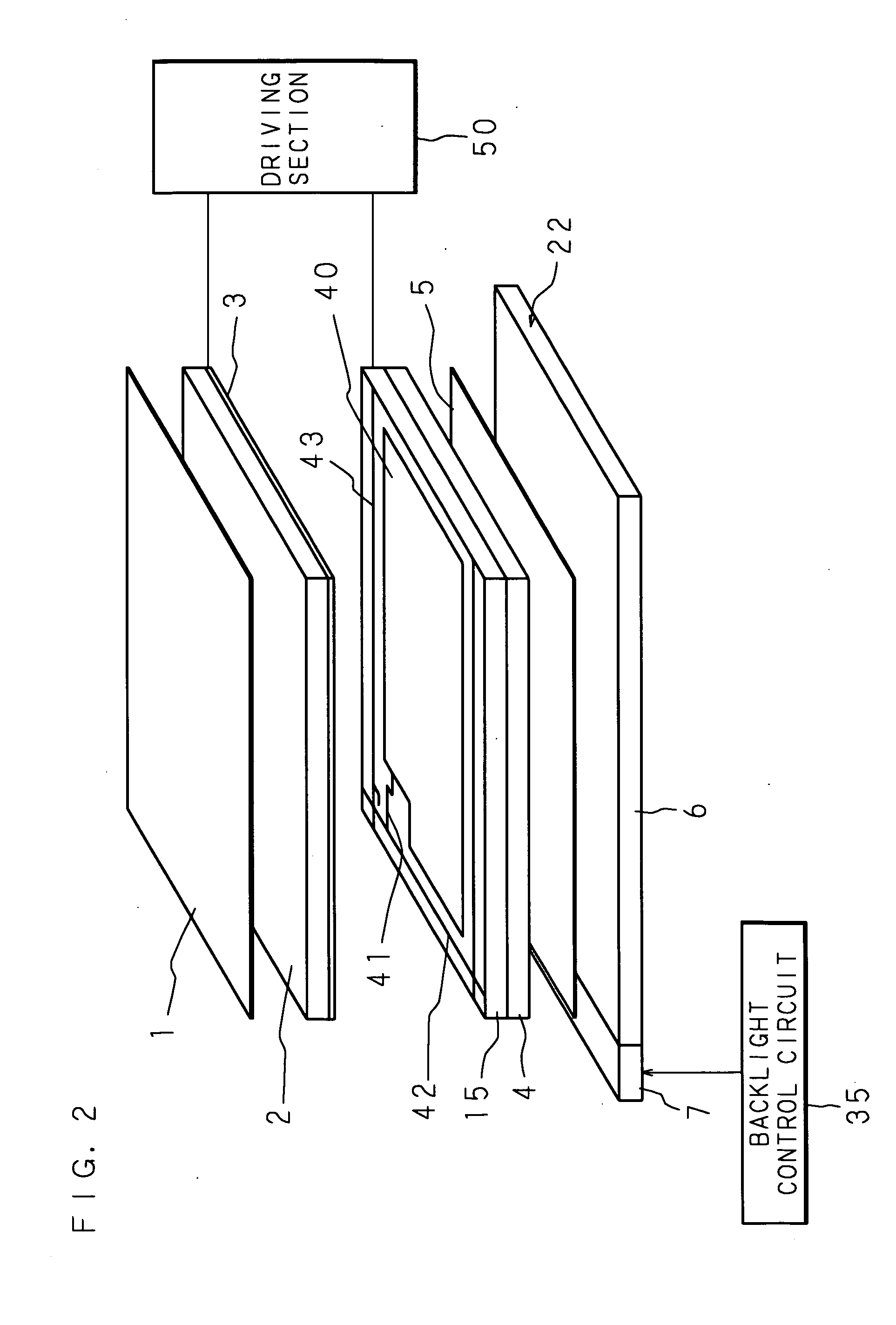
[0032]FIG. 1 is a schematic cross-sectional view showing a liquid crystal panel and a backlight according to a first embodiment of a liquid crystal display device. FIG. 2 is a schematic view showing an example of the entire structure of the liquid crystal display device. FIG. 3 is a block diagram showing a circuit structure of the liquid crystal display device. FIG. 4 is a schematic view showing an example of a structure of an LED (Light Emitting Diode) array serving as a light source for the backlight.

[0033]Reference numerals 21 and 22 indicate a liquid crystal panel and a backlight whose cross-sectional structures are shown in FIG. 1. As shown in FIGS. 1 and 2, the backlight 22 is configured by an LED array 7 and a light directing and diffusing plate 6. As shown in FIGS. 1 and 2, the liquid crystal panel 21 has a structure in which a polarizer 1, a glass substrate 2, a common electrode 3, a glass substrate 4 and a polarizer 5 are stacked in this order from the upper layer (surface...

embodiment 2

[0046]FIG. 6 is a schematic cross-sectional view showing a liquid crystal panel and a backlight according to a second embodiment of a liquid crystal display device. In FIG. 6, those parts that are the same as those shown in FIG. 1 are indicated by the same reference numerals, and the description thereof is omitted.

[0047]In the second embodiment shown in FIG. 6, as well as a flat layer 15 on the glass substrate 4, a flat layer 17 is also placed between the glass substrate 2 and the common electrode 3. With this arrangement, the thickness of the sealing member 16 is adjusted. Thus, the liquid crystal panel of the present embodiment makes it possible to satisfy the relationship of ts / tlc≧2, more preferably, ts / tlc≧3.

[0048]In the liquid crystal display having the structure as shown in FIG. 6 also, the same display driving control as that of the aforementioned liquid crystal display device shown in FIG. 1 is of course carried out.

[0049]Although not shown in the Figures, only the flat lay...

example 1

[0053]A glass substrate 4 on which pixel electrodes 40, 40 . . . (number of pixels: 640×480, length across corners: 3.2 inches) were placed with a flat layer 15 made of an acrylic material with a thickness of 2 μm being interposed therebetween and a glass substrate 2 having a common electrode 3 were washed, and these were then coated with polyimide and baked at 200° C. for one hour so that polyimide films of about 200 Å were formed as alignment films 11 and 12. Moreover, these alignment films 11 and 12 were rubbed with a cloth made from rayon, and these two substrates were superposed one on the other, with the rubbing directions being made in parallel with each other, with a gap being maintained therein by using a sealing member 16 that is made from an epoxy resin and placed on a peripheral edge portion and spacers 14 made of silica having an average particle size of 1.6 μm; thus, empty panels with a gap maintained therein were manufactured.

[0054]A ferroelectric liquid crystal mater...


PUM


Abstract

In a liquid crystal display device which has a pair of opposing substrates having a gap filled with a liquid crystal material, with a peripheral edge portion of the paired substrates being sealed by a sealing member, between the thickness (ts) of the sealing member and the thickness (tlc) of the liquid crystal layer, a relationship of ts / tlc≧2, more preferably, ts / tlc≧3, is satisfied. By making a difference smaller between a volume change in the liquid crystal material due to a temperature change and a volume change in a space in which the liquid crystal is sealed, defects caused by the volume difference are restrained from occurring. In order to achieve the relationship between ts and tlc, a flat layer is placed on one or both of the substrates.

Description

[0001]This application is Continuation Application under 35 U.S.C.§ 111(a) of PCT International Application No. PCT / JP2005 / 016649 which has an international filing date of Sep. 9, 2005 and designated the United State of America.BACKGROUND[0002]1. Technical Field[0003]The present invention relates to a liquid crystal display device, and more particularly, concerns a liquid crystal display device in which a space formed by sealing a peripheral edge portion of a pair of opposing substrates by a sealing member is filled with a liquid crystal material.[0004]2. Description of Related Art[0005]In recent years, together with developments of a so-called information society, electronic apparatuses, typically represented by personal computers, PDAs (Personal Digital Assistants) and the like, have been widely used. By the spread of these electronic apparatuses, there have been strong demands for portable apparatuses that can be used both in offices and outdoors, and small-size and light-weight ...

Claims


Application Information

Patent Timeline
IPC IPC(8): G02F1/1339
CPCG02B6/0068G02F1/1339G02F2201/50G02F2203/60G09G3/3413G09G3/3629G09G2310/0235
Inventor YOSHIHARA, TOSHIAKIMAKINO, TETSUYATADAKI, SHINJISHIROTO, HIRONORIKIYOTA, YOSHINORIBETSUI, KEIICHI
Owner FUJITSU LTD
Why Eureka
Try Eureka