Light emitting diode package having dual lens structure and backlight for liquid crystal display device implementing the same
a technology of light emitting diodes and liquid crystal displays, which is applied in the direction of optics, lighting and heating apparatus, instruments, etc., can solve the problems of increasing the cost, power consumption and heat, increasing the cost, and bulky configuration of the lcd device, and achieves efficient diffusion more widely.
- Summary
- Abstract
- Description
- Claims
- Application Information
AI Technical Summary
Benefits of technology
Problems solved by technology
Method used
Image
Examples
second embodiment
[0102]FIG. 9 is a cross-sectional view showing an LED package of an LCD device in accordance with the present invention.
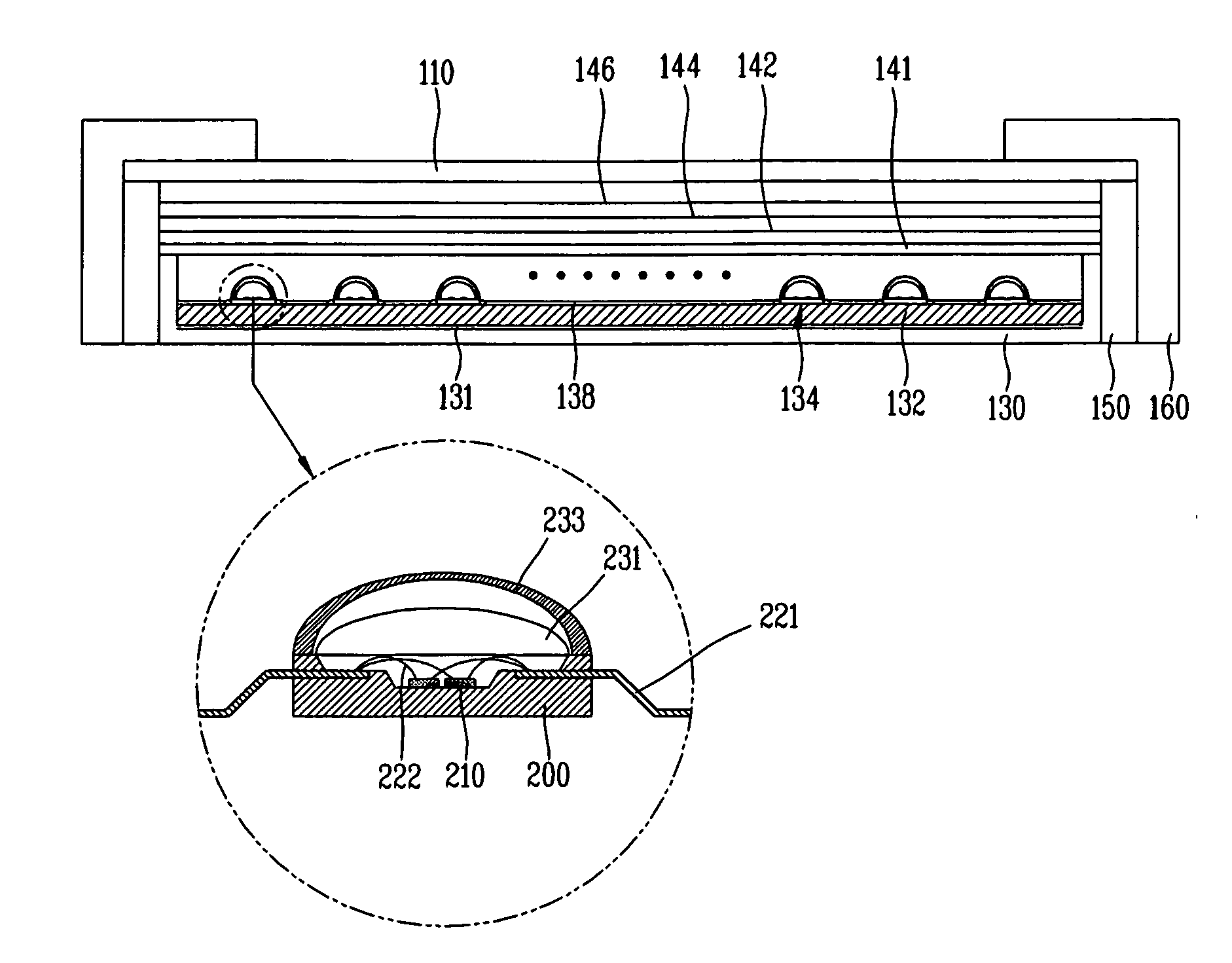
[0103]As compared with FIGS. 4 and 5, the LED package according to the second embodiment of the present invention includes a main body 400 implementing a periphery with a recess in its central portion, R, G and B LED chips 410 mounted in the recess in the main body 400, respective conducting terminals 421 and 422 connected to the R, G and B LED chips 410 to apply voltages thereto, a first lens 431 formed on the LED chips 410 and having a first curvature which is gradually increased from its edge portion toward its central portion, and a second lens 433 formed at the edge and the central portion of the first lens 431 wherein its inner curved surface has a second curvature which is gradually increased from the edge portion toward the central portion and its outer curved surface has a third curvature which is gradually decreased from the edge portion toward the centra...
first embodiment
[0107]Now, although not shown in any additional drawing, an LED package of a backlight for an LCD device which is a variation of the present invention will be described.
[0108]As compared with FIGS. 4 and 5, the LED package of the backlight for the LCD device according to the present invention includes a main body implementing a periphery with a recess in its central area, R, G and B LED chips mounted in the recess in the main body, conducting terminals connected to the R, G and B LED chips to apply voltages thereto, a first lens formed on the LED chips and having a first curvature, and a second lens formed at the edge and the central portion of the first lens, wherein its inner curved surface has a second curvature which is gradually increased from the edge portion toward the central portion and its outer curved surface has a third curvature which is gradually decreased from the edge portion toward the central portion.
[0109]That is, the third curvature of the outer curved surface of...
PUM
| Property | Measurement | Unit |
|---|---|---|
| optical reflectivity | aaaaa | aaaaa |
| inclination angle | aaaaa | aaaaa |
| inclination angle | aaaaa | aaaaa |
Abstract
Description
Claims
Application Information


