

System debug and trace system and method, and applications thereof
- Summary
- Abstract
- Description
- Claims
- Application Information
AI Technical Summary
Benefits of technology
Problems solved by technology
Method used
Image

Examples
Embodiment Construction
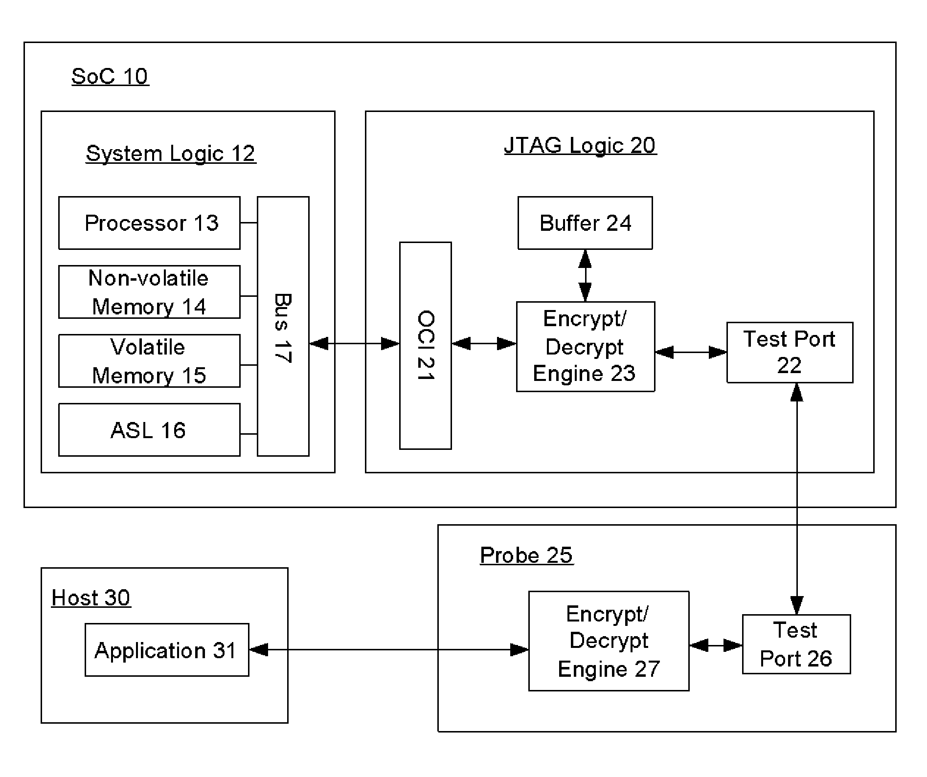
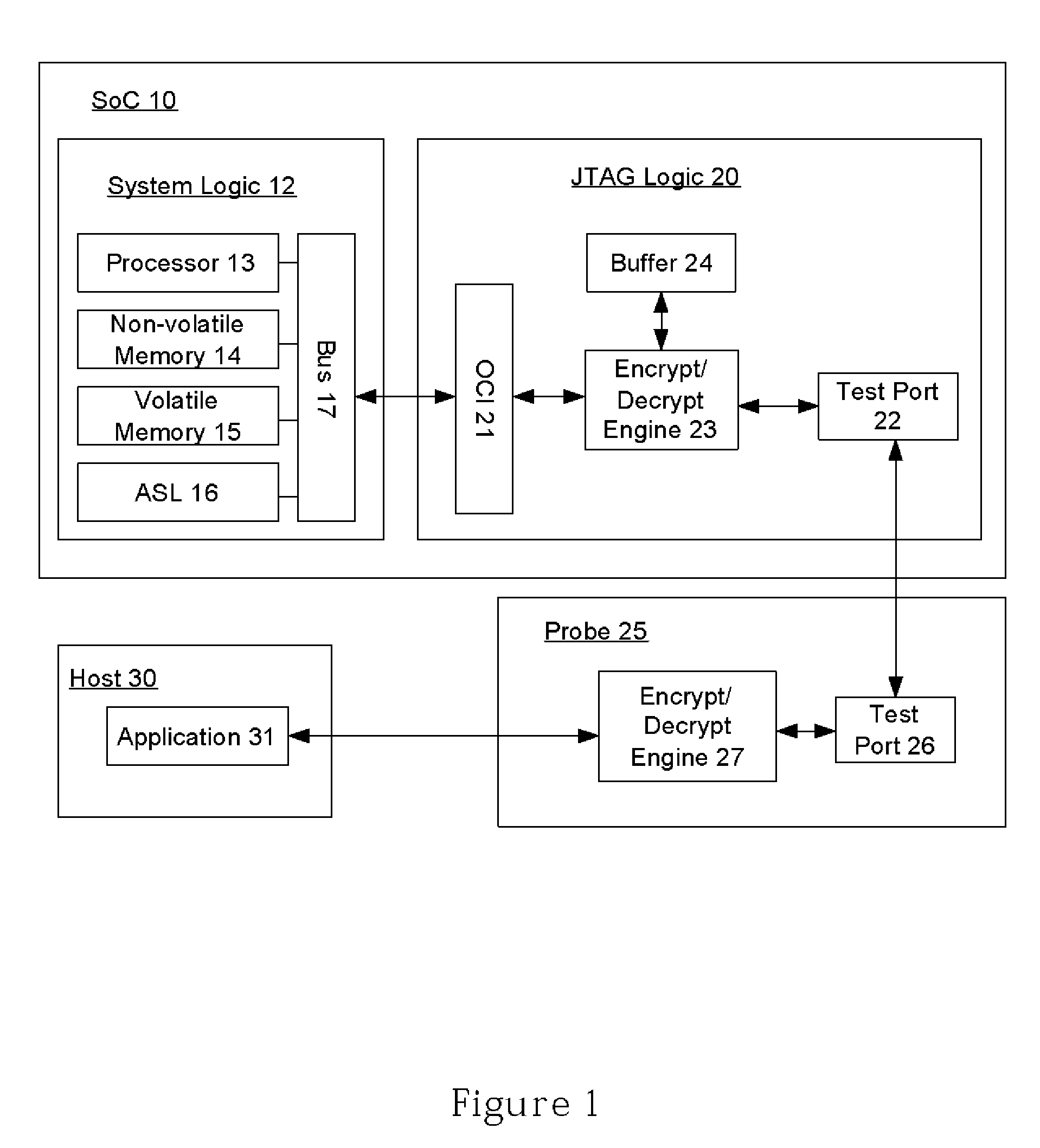
[0022]A preferred embodiment of the invention is now described with reference to the figures where like reference numbers illustrate like elements. While specific methods and configurations are discussed, it should be understood that this is done for illustration purposes only. A person skilled in the relevant art will recognize that other components, configurations and procedures may be used without departing from the spirit and scope of the invention.
[0023]In one embodiment, a system and method provide secure on-chip control, capture, and export of debug and trace information in an embedded environment. An on-chip mechanism provides test, debug and trace information to a test probe. One exemplary test mechanism utilizes a Joint Test Action Group (“JTAG”) test access port (“TAP”) as defined in IEEE Standard 1149.1, IEEE Standard Test Access Port and Boundary-Scan Architecture (the “IEEE Standard”) that is combined with encryption and decryption logic to render traffic unreadable wi...
PUM
 Abstract
Description
Claims
Application Information