

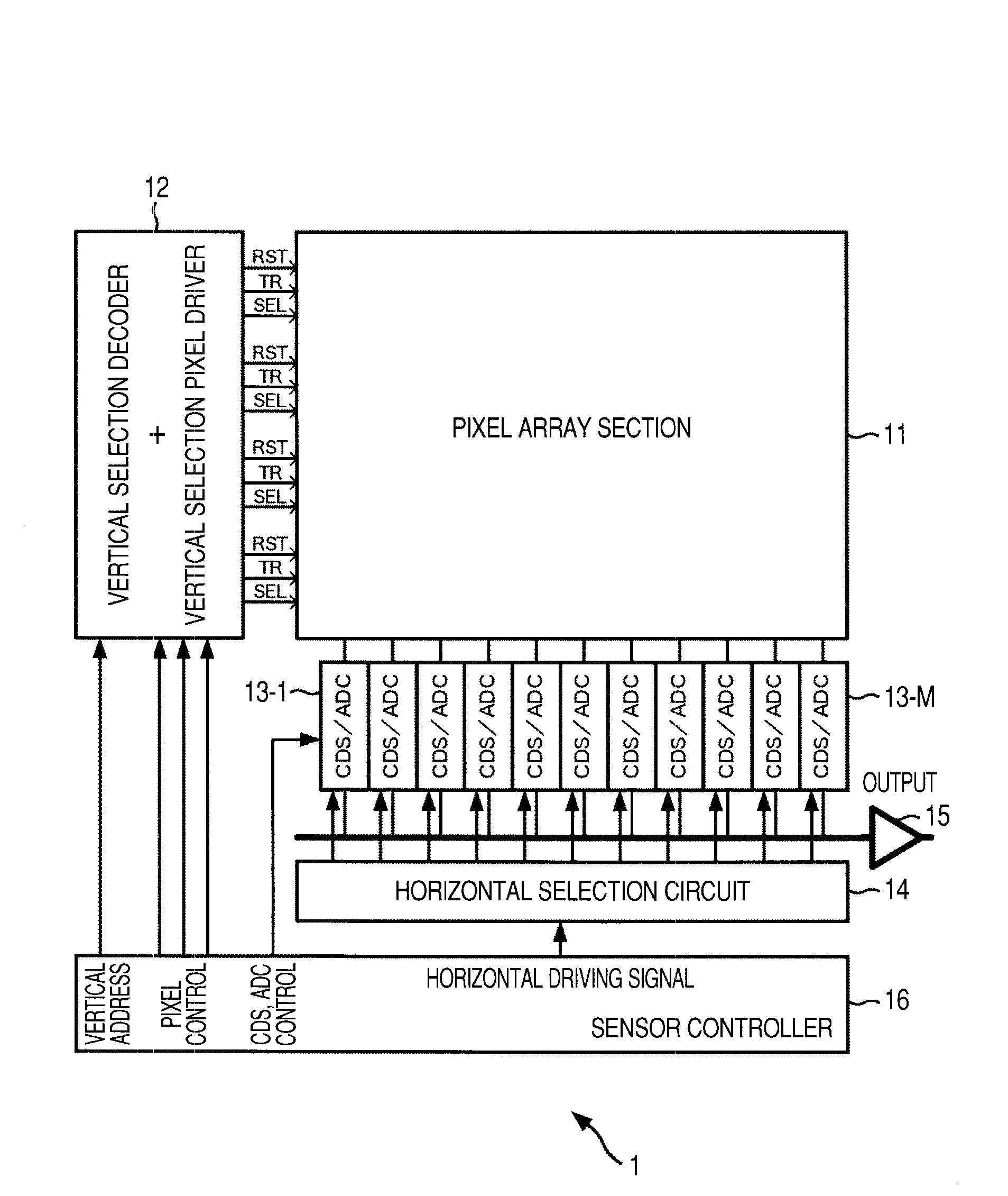
Image sensor, electronic apparatus, and driving method of electronic apparatus
a technology of electronic equipment and image sensor, applied in the field of image sensor, can solve the problems of not being able not being able to provide a switch for avoiding blooming, and not being able to miniaturize the pixel, so as to reduce the gate size and chip size. , the effect of simple configuration
- Summary
- Abstract
- Description
- Claims
- Application Information
AI Technical Summary
Benefits of technology
Problems solved by technology
Method used
Image

Examples
first embodiment
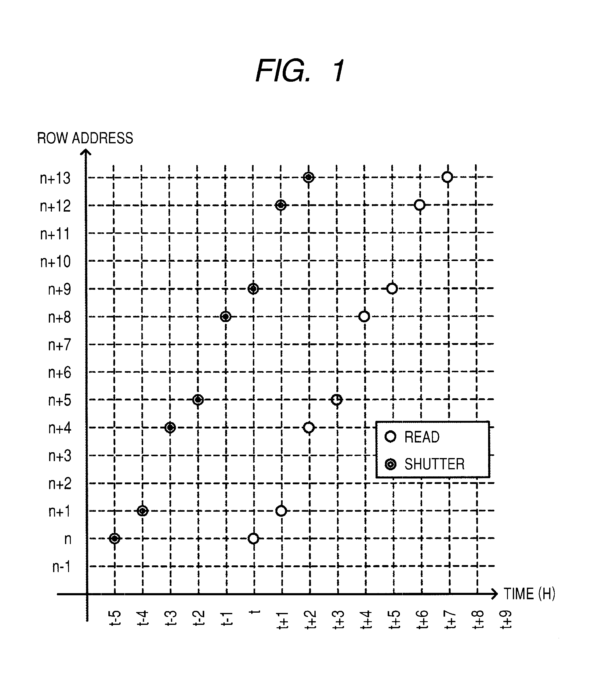
[0100]FIG. 6 shows a first embodiment of a control of the electronic shutter occurrence number made by the sensor controller 16.
[0101]FIG. 6 illustrates an example in which a pre-shutter, which is a shutter having a function of suppressing blooming onto a row (object row for the exposure regulation shutter) on which the exposure regulation shutter is executed, is executed on the V selection circuit 12 in addition to the exposure regulation shutter in the case when the address addition amount (1) is designated from the DSP 51, that is, in the case when the image sensor 1 performs all pixel reading.
[0102]Similar to the case shown in FIG. 4, FIG. 6 illustrates an example in which the image sensor 1 performs all pixel reading with an accumulation time 3 [H].
[0103]In FIG. 6, for example, an exposure regulation shutter of a row address n read at time (t+3) [H] is executed at time t [H], but the V selection circuit 12 executes a pre-shutter on a row address (n+1) together with the exposure...
second embodiment
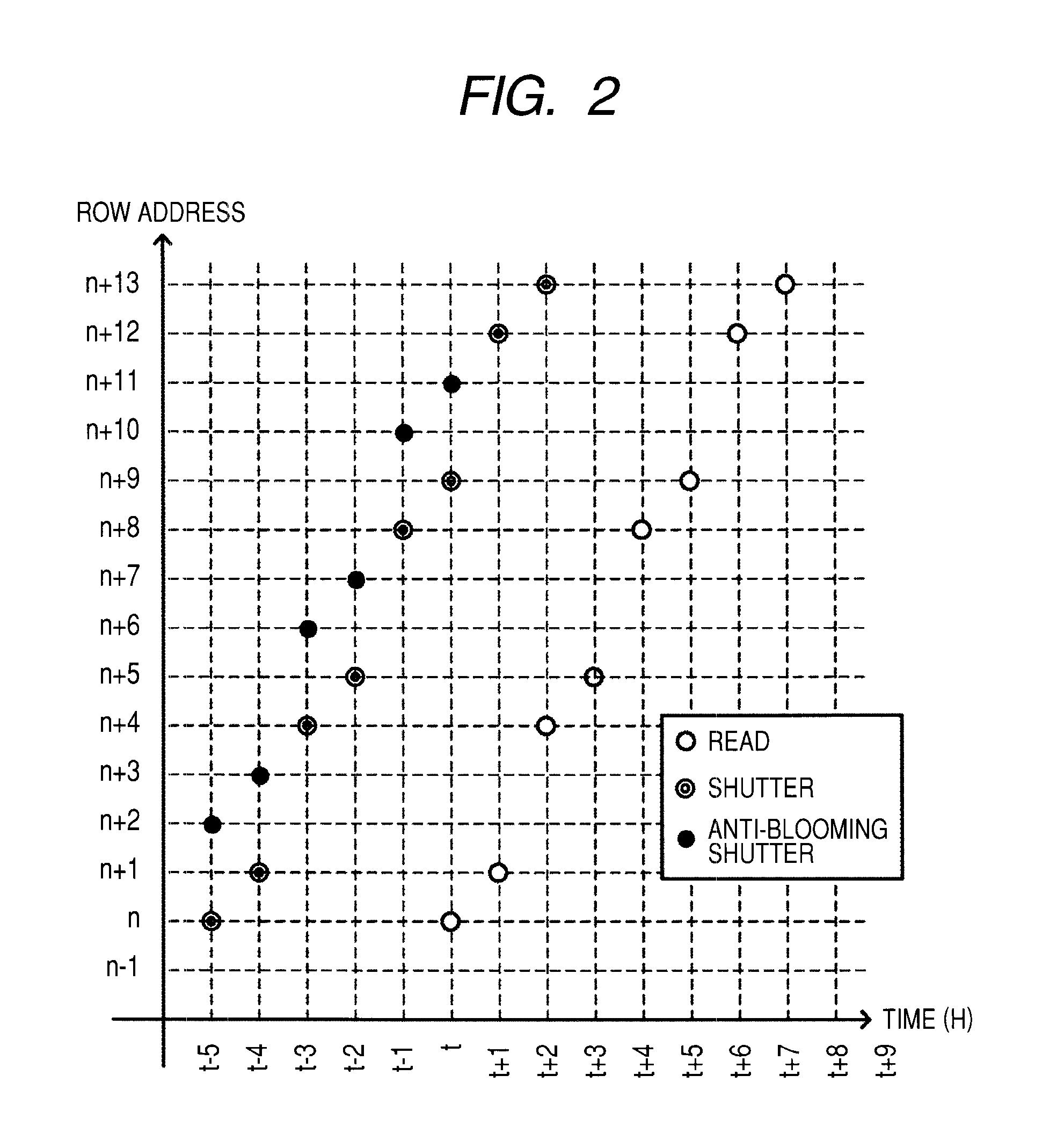
[0117]FIG. 8 shows a second embodiment of a control of the electronic shutter occurrence number made by the sensor controller 16.
[0118]In the second embodiment, the sensor controller 16 determines the electronic shutter occurrence number within one horizontal scanning period on the basis of a maximum value of an absolute value of each of the address addition amounts P1, P2, P3, . . . , PN when the address addition amount (P1, P2, P3, . . . , PN) is designated from the DSP 51.
[0119]More specifically, assuming that the maximum value of the absolute value of each of the address addition amounts P1, P2, P3, . . . , PN is Q, the sensor controller 16 sets the electronic shutter occurrence number within one horizontal scanning period to Q or more and performs an electronic shutter on rows of Q or more continuous row addresses with a row address of an object row for an exposure regulation shutter as a reference.
[0120]The number of rows on which an anti-blooming shutter is operated in one ho...
third embodiment
[0124]FIG. 9 shows a third embodiment of a control of the electronic shutter occurrence number made by the sensor controller 16.
[0125]In the third embodiment, the sensor controller 16 determines the electronic shutter occurrence number within one horizontal scanning period on the basis of a maximum value of an absolute value of each of the nearest-neighbor addition amounts P1+P2, P2+P3, P3+P4, . . . , PN−1+PN, PN+P1, which are obtained by adding address addition amounts of rows adjacent to each other, when the address addition amount (P1, P2, P3, . . . , PN) is designated from the DSP 51.
[0126]More specifically, assuming that the maximum value of the absolute value of each of the nearest-neighbor addition amounts P1+P2, P2+P3, P3+P4, . . . , PN−1+PN, PN+P1 is R, the sensor controller 16 sets the electronic shutter occurrence number within one horizontal scanning period to R / 2 or more and performs an electronic shutter on rows of R / 2 or more discontinuous row addresses with every oth...
PUM
 Abstract
Description
Claims
Application Information