

Method for fabricating metal pad
a metal pad and fabrication method technology, applied in the direction of basic electric elements, electrical equipment, semiconductor devices, etc., can solve the problems of cracks or voids formed on the lower insulation film, and the technique is not without problems, so as to improve the bonding force between the via contact and the metal pad. , the effect of preventing the formation of cracks
- Summary
- Abstract
- Description
- Claims
- Application Information
AI Technical Summary
Benefits of technology
Problems solved by technology
Method used
Image

Examples
Embodiment Construction
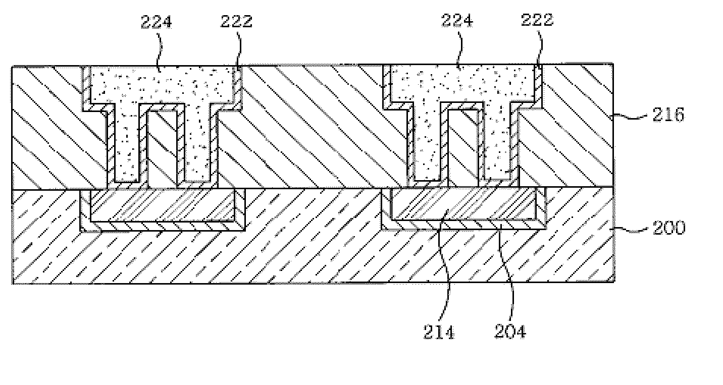
[0008]In general, example embodiments of the of the present invention relate to methods for fabricating a metal pad in a manner so as to minimize or prevent connection defects between via contacts and the metal pad. In this way, the bonding force between a via contact and a metal pad is improved.
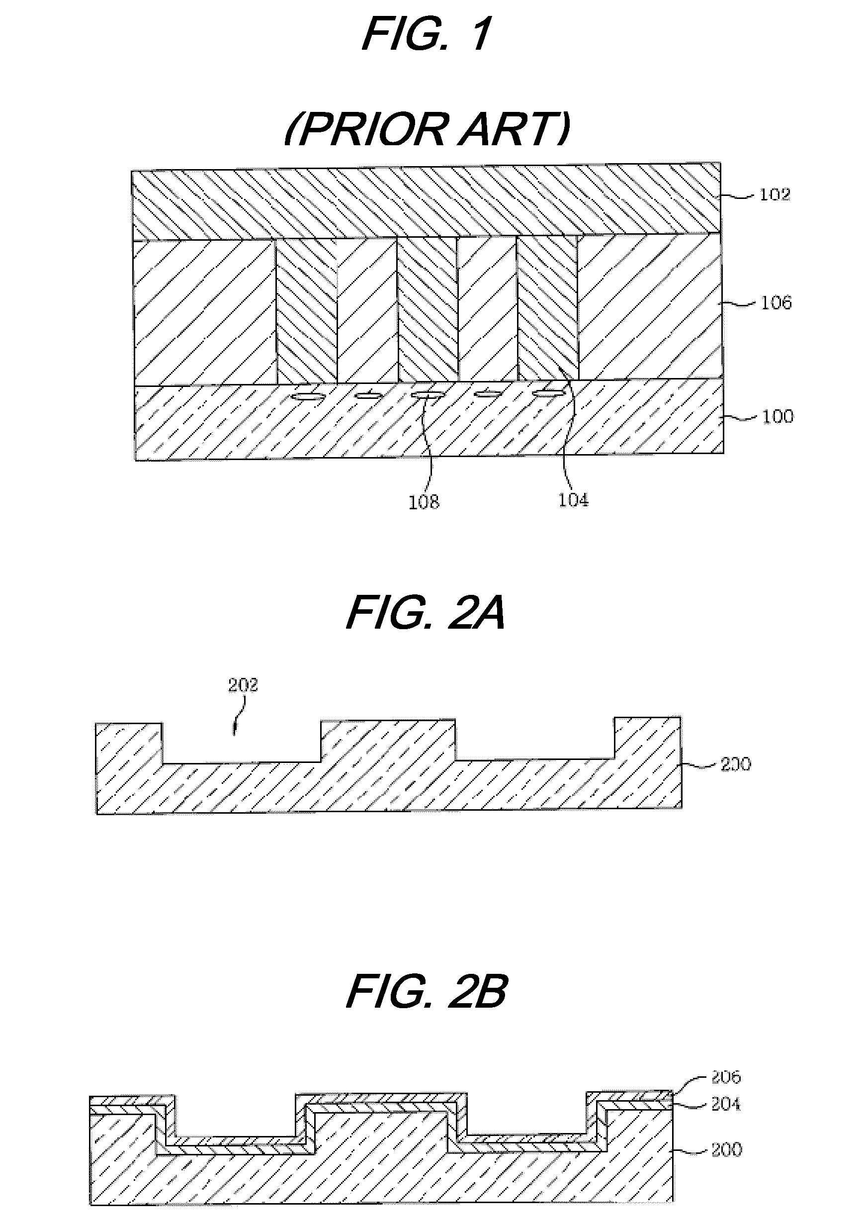
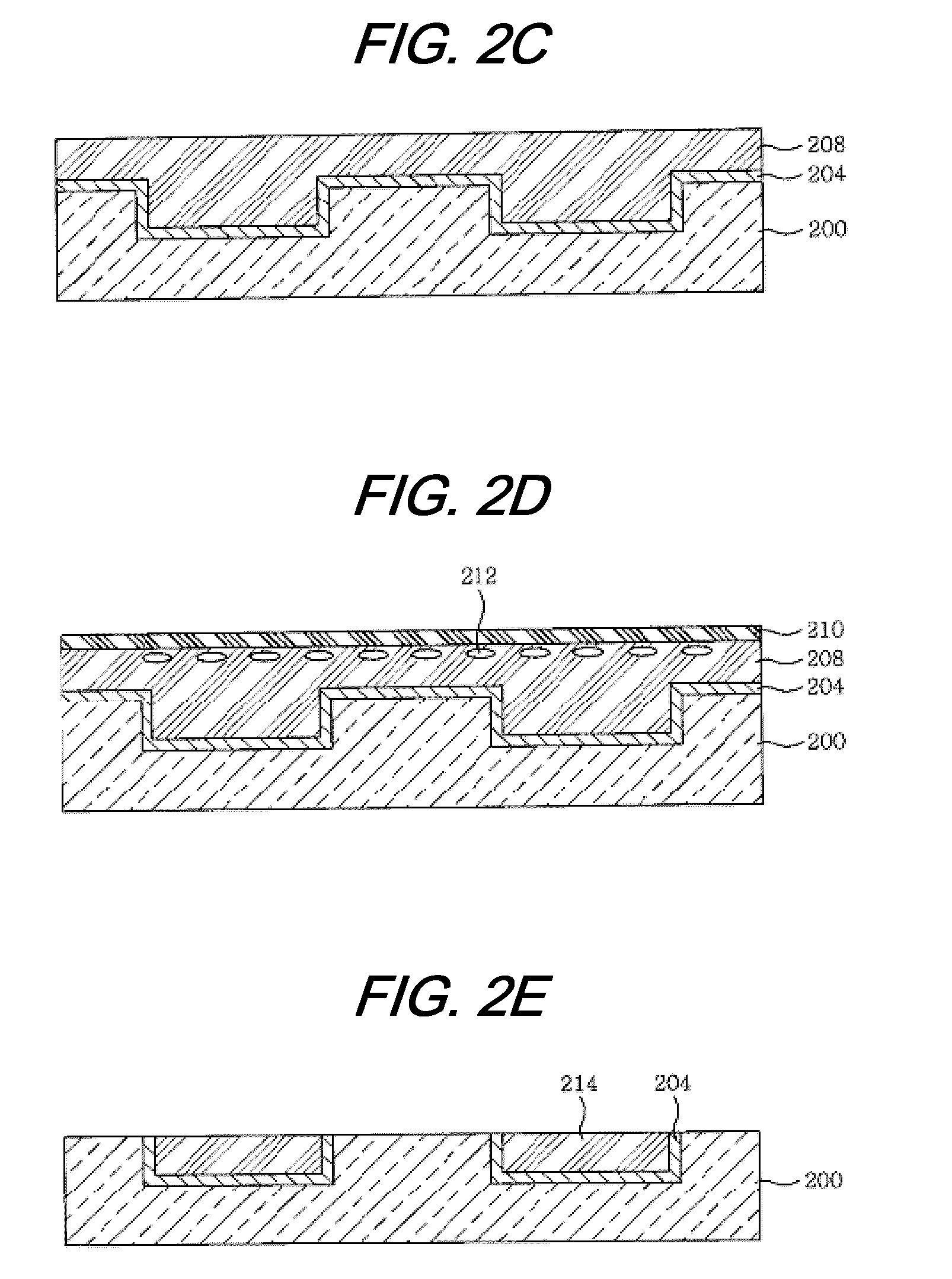
[0009]In accordance with one example embodiment, a fabrication method includes the step of selectively etching a wire insulation film formed on a semiconductor substrate to form a pattern, such as a dual damascene pattern, having plural vias in one trench. A metal film is deposited to fill the pattern. An insulation film is formed on the metal film, which produces stress between the metal film and the insulation film such that voids are formed inside the metal film or between the metal film and the insulation film. The voids created from the stress are concentrated at the upper portion of the metal film. The insulation film and the metal film can then be removed to expose a surface of the wi...
PUM
 Abstract
Description
Claims
Application Information