Coreless packaging substrate and method of fabricating the same

a packaging substrate and coreless technology, applied in the direction of semiconductor devices, electrical equipment, semiconductor/solid-state device details, etc., can solve the problems of increasing the thickness of the overall structure, increasing the difficulty of the process, weakening the bonding force, etc., to achieve the effect of reducing the distance between metal bumps, simple manufacturing of packaging substrates, and not prone to falling off and being damaged

Active Publication Date: 2016-04-21
UNIMICRON TECH CORP
View PDF0 Cites 2 Cited by
  • Summary
  • Abstract
  • Description
  • Claims
  • Application Information

AI Technical Summary

Benefits of technology

The present invention provides a method for manufacturing semiconductor chips with metal bumps that are exposed from a dielectric passivation layer. This method avoids the problem of alignment between solder balls and openings in the conventional technique, simplifies the manufacturing process of packaging substrates, and increases the bonding force between the metal bumps and semiconductor chip, reducing the likelihood of damage. Additionally, the smaller area of the metal bumps allows for a greater number of metal bumps to be packed into a smaller space, improving the layout density of the metal bumps.

Problems solved by technology

The use of the core board causes the overall structure to have an increased thickness, which is contradictory to the requirements of increasing performance and reducing sizes.
Although it is necessary in the conventional packaging substrate 1 to form the openings 140a and 140b on the solder masks 14a and 14b, the alignment between the solder balls 15a and 15b and the openings 140a and 140b is not easy, thus increasing the difficulty of the process.
Furthermore, the openings 140b of the solder mask 14b only expose a part of the top surface of each of the second electrical pads 123, rather than the entire top surface, so that the area of the top surface of each of the metal bumps 13b is reduced, resulting in weakening of the bonding force between the metal bumps 13b and the chip at the time the chip is installed on the packaging substrate 1, thereby making the chips easily fallen off from the packaging substrate 1 and damaged.

Method used


Image

  • Coreless packaging substrate and method of fabricating the same
  • Coreless packaging substrate and method of fabricating the same
  • Coreless packaging substrate and method of fabricating the same

Examples


Embodiment Construction

[0021]It is to be understood that both the foregoing general descriptions and the following detailed embodiments are exemplary and are, together with the accompanying drawings, intended only to provide further explanation of technical features and advantages of the invention.

[0022]The following illustrative embodiments are provided to illustrate the disclosure of the present invention, these and other advantages and effects can be apparent to those skilled in the art after reading the disclosure of this specification. The present invention can also be performed or applied by other different embodiments. The details of the specification may be on the basis of different points and applications, and numerous modifications and variations can be devised without departing from the spirit of the present invention.

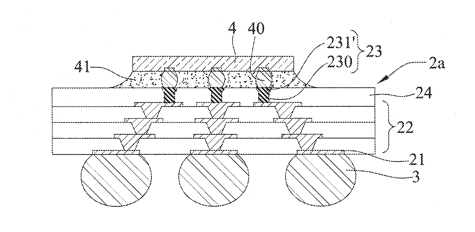
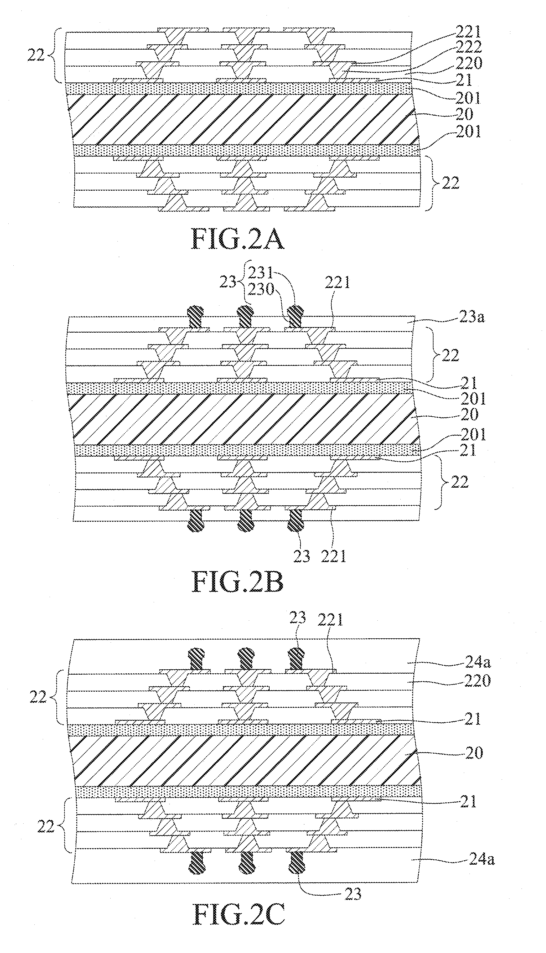
[0023]FIGS. 2A to 2E are schematic cross-sectional views illustrating a method of fabricating a coreless packaging substrate according to the present invention.

[0024]As shown in F...


PUM


Abstract

A coreless packaging substrate includes: a circuit buildup structure having at least a dielectric layer, a wiring layer and a plurality of conductive elements, a plurality of electrical pads embedded in the dielectric layer of the circuit buildup structure, a plurality of metal bumps formed on the wiring layer of the circuit buildup structure, and a dielectric passivation layer formed on the surface of the circuit buildup structure and the metal bumps with the metal bumps exposed from the dielectric passivation layer. The metal bumps each have a metal column portion and a wing portion integrally connected to the metal column portion, such that the bonding force between the metal bumps and a semiconductor chip can be enhanced by the entire top surface of the wing portions of the metal bumps being completely exposed.

Description

RELATED APPLICATIONS[0001]The present application is a Divisional application of U.S. application Ser. No. 13 / 417,858, filed on Mar. 12, 2012, which claims priority of Taiwan Application Serial Number 100124353, filed on Jul. 8, 2011, all of which are herein incorporated by reference.BACKGROUND[0002]1. Technical Field[0003]The present invention relates generally to packaging substrates, and, more particularly, to a coreless packaging substrate and a method of fabricating the same.[0004]2. Description of Related Art[0005]With the rapid development of electronic industry, electronic products are trending toward multi-function and high-performance. Currently, the semiconductor package structure has developed various package types such as wire bonding or flip chip that forms a semiconductor chip on a packaging substrate, and the semiconductor chip electrically connects to the packaging substrate by bonding wires or solder bumps. In order to meet the packaging requirements of high integr...

Claims


Application Information

Patent Timeline
Patent Type & Authority Applications(United States)
IPC IPC(8): H01L21/48H01L21/683
CPCH01L21/4857H01L21/4853H01L2221/6835H01L21/6835H01L21/486H01L23/49816H01L23/49822H01L23/49827H01L24/16H01L2224/131H01L2224/16225H01L2224/16237H01L2224/32225H01L2224/73204H01L2224/83102H01L2924/12042H01L2924/15311
Inventor TSENG, TZYY-JANGHO, CHUNG-W.
Owner UNIMICRON TECH CORP
Why Eureka
Try Eureka