Organic electroluminescence device and method for manufacture thereof

a technology of electroluminescent devices and manufacturing methods, which is applied in the direction of thermoelectric devices, solid-state devices, and nano-informatics. it can solve the problems of affecting the stability of the oled device, the morphology of the conductive film is not controllable, and the carrier and transmission performance is not controllable, so as to improve the bonding force between the anode and the substrate, the effect of superior light transmittance and low surface resistan

Inactive Publication Date: 2014-11-13
OCEANS KING LIGHTING SCI&TECH CO LTD +1
View PDF6 Cites 1 Cited by
  • Summary
  • Abstract
  • Description
  • Claims
  • Application Information

AI Technical Summary

Benefits of technology

[0020]The organic electroluminescence device manufactured by vacuum vapor deposition and dip-coating process has stacked structure anode. The stacked structure of anode only causes minor damage to substrate. The anode has superior light transmittance and low surface resistance. The bonding force between the anode and the substrate is enhanced by inserting buffer layer. The device has a stable luminous property and a high luminous efficiency.

Problems solved by technology

However, such conductive film has many insurmountable problems in application for flexible OLED.
For example, in the process of preparing ITO film, the doping proportion of various elements, such as indium and stannum, is difficult to control, resulting in uncontrollable morphology of ITO, carrier and transmission performance.
The prepared conductive film has high surface resistance, weak bonding force between the film and the substrate, so that the conductive film is prone to falling off the substrate in the process of repeated bending, thus affecting the stability of the OLED device.

Method used


Image

  • Organic electroluminescence device and method for manufacture thereof
  • Organic electroluminescence device and method for manufacture thereof
  • Organic electroluminescence device and method for manufacture thereof

Examples


example 1

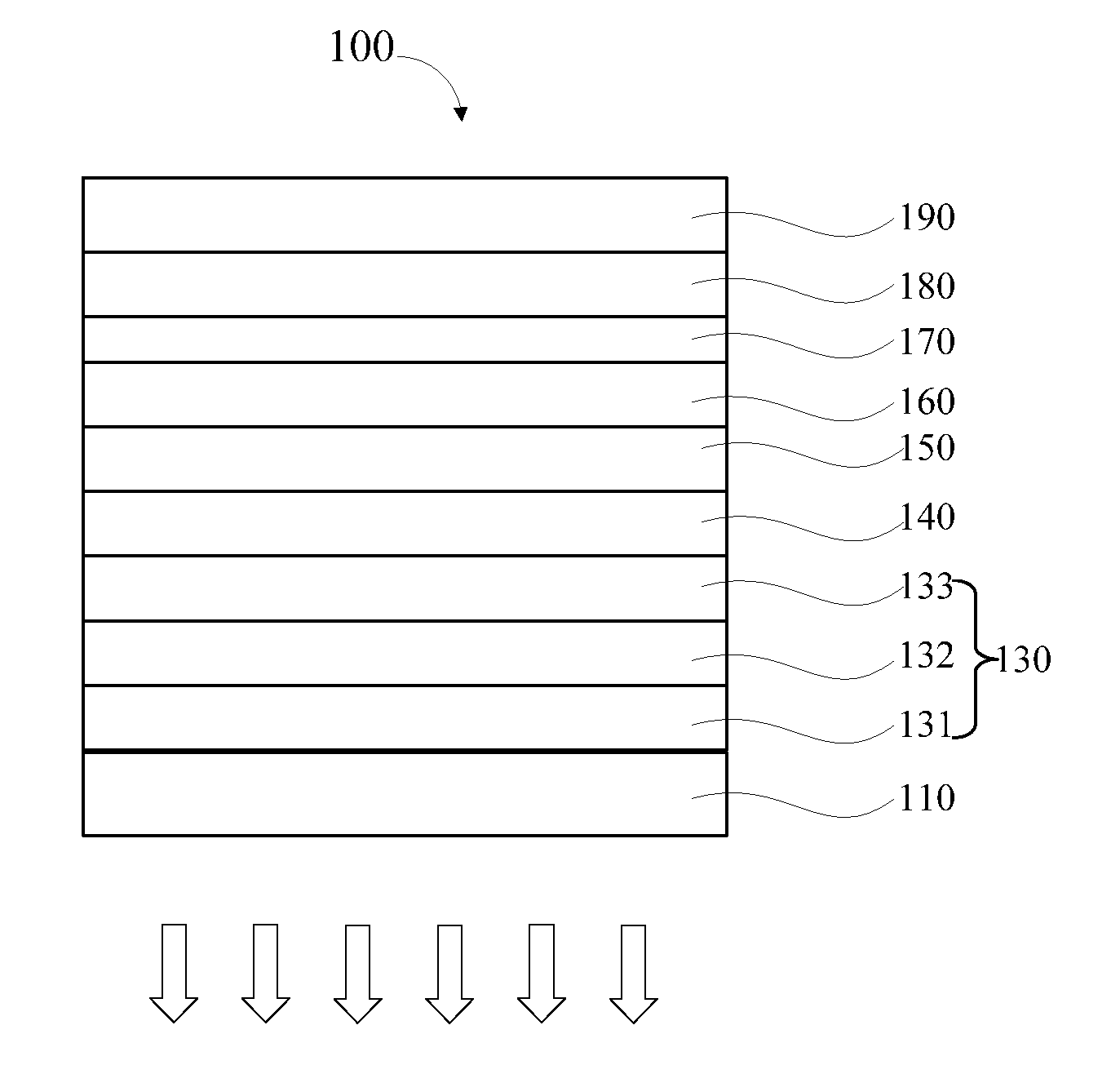
[0076]The method for manufacturing organic electroluminescent device is as follows.

[0077]Preparation of substrate. Polyethylene naphthalate film having a thickness of 0.1 mm was ultrasonically cleaned in deionized water containing detergent, washed with deionized water, ultrasonically treated successively with isopropanol and acetone, then blow dried with nitrogen.

[0078]Preparation of buffer layer. The dried substrate was placed on a spin coater. Speed of the spin coater was set for 1000 r / min. The spin coater started and operated for 120 s. An ultraviolet light curing adhesive of 0.5 nm thick was coated on the surface of substrate. Then a UV lamp was employed to cure to form a buffer layer. Surface hardness of the buffer layer was 2H.

[0079]Preparation of anode. A light transmittance increased layer was deposited on the surface of buffer layer in a vacuum depositing system at 5×10⁻⁴ Pa, then taken out from the vacuum depositing system. In this embodiment, zinc sulfide layer having a...

example 2

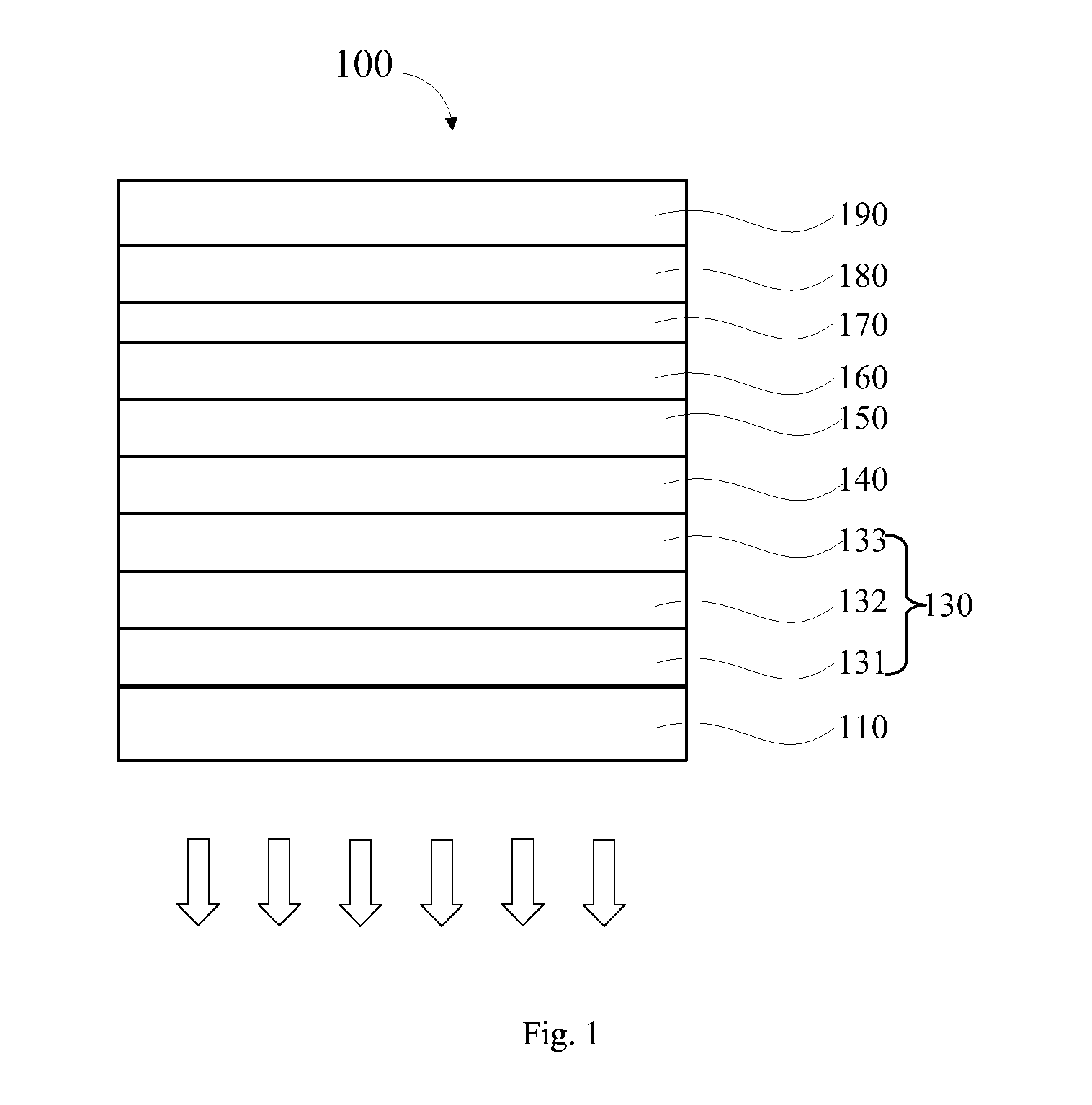
[0091]The method for manufacturing organic electroluminescent device is as follows.

[0092]Preparation of substrate. Polyethylene terephthalate film having a thickness of 0.175 mm was ultrasonically cleaned in deionized water containing detergent, washed with deionized water, ultrasonically treated successively with isopropanol and acetone, then blow dried with nitrogen;

[0093]Preparation of buffer layer. The dried substrate was placed on a spin coater. Speed of the spin coater was set for 5000 r / min. The spin coater started and operated for 30 s. An ultraviolet light curing adhesive of 5 μm thick was coated on the surface of substrate. Then a UV lamp was employed to cure to form a buffer layer. Surface hardness of the buffer layer was 3H.

[0094]Preparation of anode. A light transmittance increased layer was deposited on the surface of buffer layer in a vacuum depositing system at 5×10⁻⁴ Pa, then taken out from the vacuum depositing system. In this embodiment, zinc sulfide layer having ...

example 3

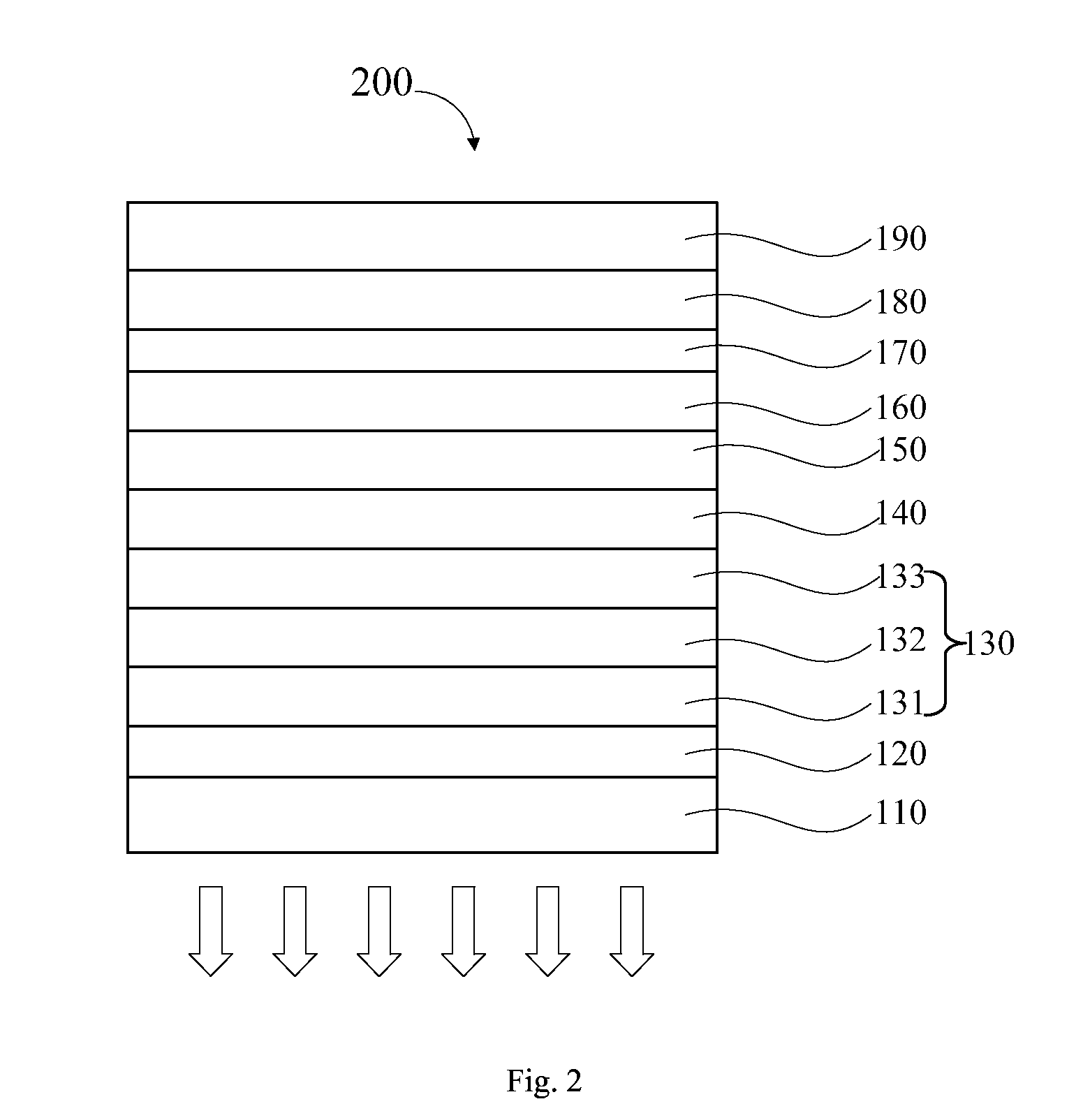
[0105]The method for manufacturing organic electroluminescent device is as follows.

[0106]Preparation of substrate. Polyether sulfone film having a thickness of 0.2 mm was ultrasonically cleaned in deionized water containing detergent, washed with deionized water, ultrasonically treated successively with isopropanol and acetone, then blow dried with nitrogen;

[0107]Preparation of buffer layer. The dried substrate was placed on a spin coater. Speed of the spin coater was set for 4000 r / min. The spin coater started and operated for 70 s. An ultraviolet light curing adhesive of 1 μm thick was coated on the surface of substrate. Then a UV lamp was employed to cure to form a buffer layer. Surface hardness of the buffer layer was 2H.

[0108]Preparation of anode. A light transmittance increased layer was deposited on the surface of buffer layer in a vacuum depositing system at 5×10⁻⁴ Pa, then taken out from the vacuum depositing system. In this embodiment, zinc sulfide layer having a thickness...


PUM


Abstract

An organic electroluminescence device (100, 200) comprises a substrate (110), an anode (130), a light emitting layer (160) and a cathode (190) stacked sequentially. The anode (130) comprises a light transmittance increased layer (131), a conductive layer (132) and a hole injection auxiliary layer (133) stacked on the substrate (110) sequentially. The materials of the light transmittance increased layer (131) are inorganic compounds of zinc with a light transmittance of 400 nm to 800 nm in the visible region and a refractive index greater than 2.3. The material of the conductive layer (132) is graphene. The utilization of light transmittance increased principle for multilayer anode structure can make the light transmittance of the anode in the visible region high and surface resistance low. The utilization of inorganic material with hole injection ability can reduce the hole injection barrier, make the luminous performance of the organic electroluminescence device (100, 200) stable and luminous efficiency high. A method for manufacturing the organic electroluminescence device (100, 200) is also provided. The anode is prepared by vacuum evaporation and pulling method, which is convenient to operate and is suitable for large scale production.

Description

FIELD OF THE INVENTION[0001]The present invention relates to an organic electroluminescent device and manufacturing method thereof.BACKGROUND OF THE INVENTION[0002]Organic light emitting diode, hereinafter referred to as OLED, a promising display technique and light source, has characteristics such as high luminance, wide selection of material, low driving voltage and solid-state self-luminosity, as well as advantages such as high definition, wide viewing angle and fast response. OLED not only conforms to the development trends of mobile communication and information display in the information age, but also meets the requirements of green lighting technology, and has drawn considerable attention of many researchers at home and abroad.[0003]Organic light emitting diode has a similar sandwich structure, comprising cathode and anode positioned separately on the top and the bottom, and one or more functional layers of organic materials sandwiched between the electrodes. The functional l...

Claims


Application Information

Patent Timeline
Patent Type & Authority Applications(United States)
IPC IPC(8): H01L51/50H01L51/00
CPCH01L51/5024H01L51/0001H01L2251/56B82Y10/00H10K85/20H10K50/858H10K71/60H10K50/816H10K50/12H10K71/00
Inventor ZHOU, MINGJIEWANG, PINGFENG, XIAOMINGCHEN, JIXING
Owner OCEANS KING LIGHTING SCI&TECH CO LTD
Why Eureka
Try Eureka