Method of manufacturing chip integrated substrate

a technology of integrated substrates and manufacturing methods, applied in the manufacture of printed circuits, printed circuit aspects, basic electric elements, etc., can solve the problems of short circuit generation between adjacent wires, and achieve the effect of enhancing the reliability of the chip integrated substrate and preventing a breakage or a short circuit of the wir

Active Publication Date: 2008-11-27
SHINKO ELECTRIC IND CO LTD
View PDF7 Cites 7 Cited by
  • Summary
  • Abstract
  • Description
  • Claims
  • Application Information

AI Technical Summary

Benefits of technology

[0011]In consideration of the respects, it is an object of the invention to provide a method of manufacturing a chip integrated substrate which can maintain a high reliability even if a chip component is connected to a first substrate through a wire.
[0018]According to the invention, the chip component connected to the first substrate through the wire and the wire are sealed with the first resin by using the molding tool before the connecting pad and the electrode are bonded to each other through the solder. Even if flux cleaning is carried out after the connecting pad and the electrode are bonded to each other through the solder, therefore, it is possible to prevent a breakage or a short circuit of the wire from being generated in the flux cleaning. Accordingly, it is possible to enhance a reliability of the chip integrated substrate.

Problems solved by technology

In the case in which the solder flux remains as a residue after the soldering, it causes a corrosion.
In this case, there is a problem in that the wire is broken or the wire is deformed, resulting in the generation of a short circuit between adjacent wires.

Method used


Image

  • Method of manufacturing chip integrated substrate
  • Method of manufacturing chip integrated substrate
  • Method of manufacturing chip integrated substrate

Examples


Embodiment Construction

[0021]Next, the best mode for carrying out the invention will be described with reference to the drawings.

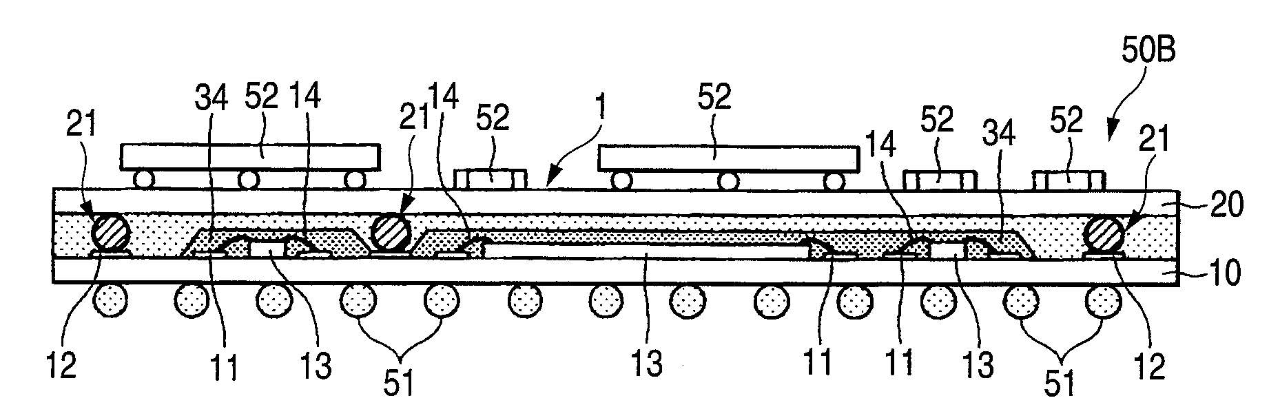
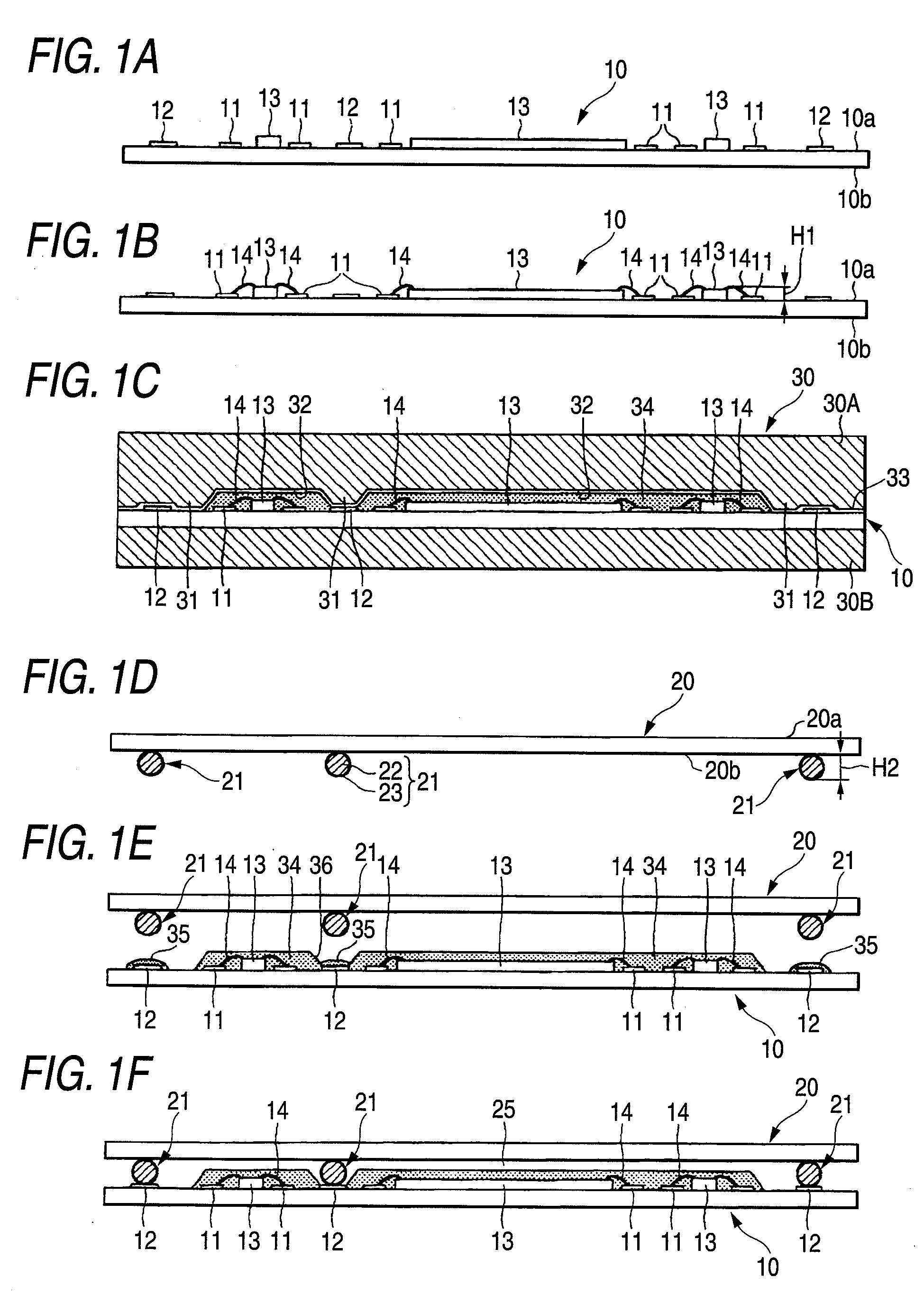
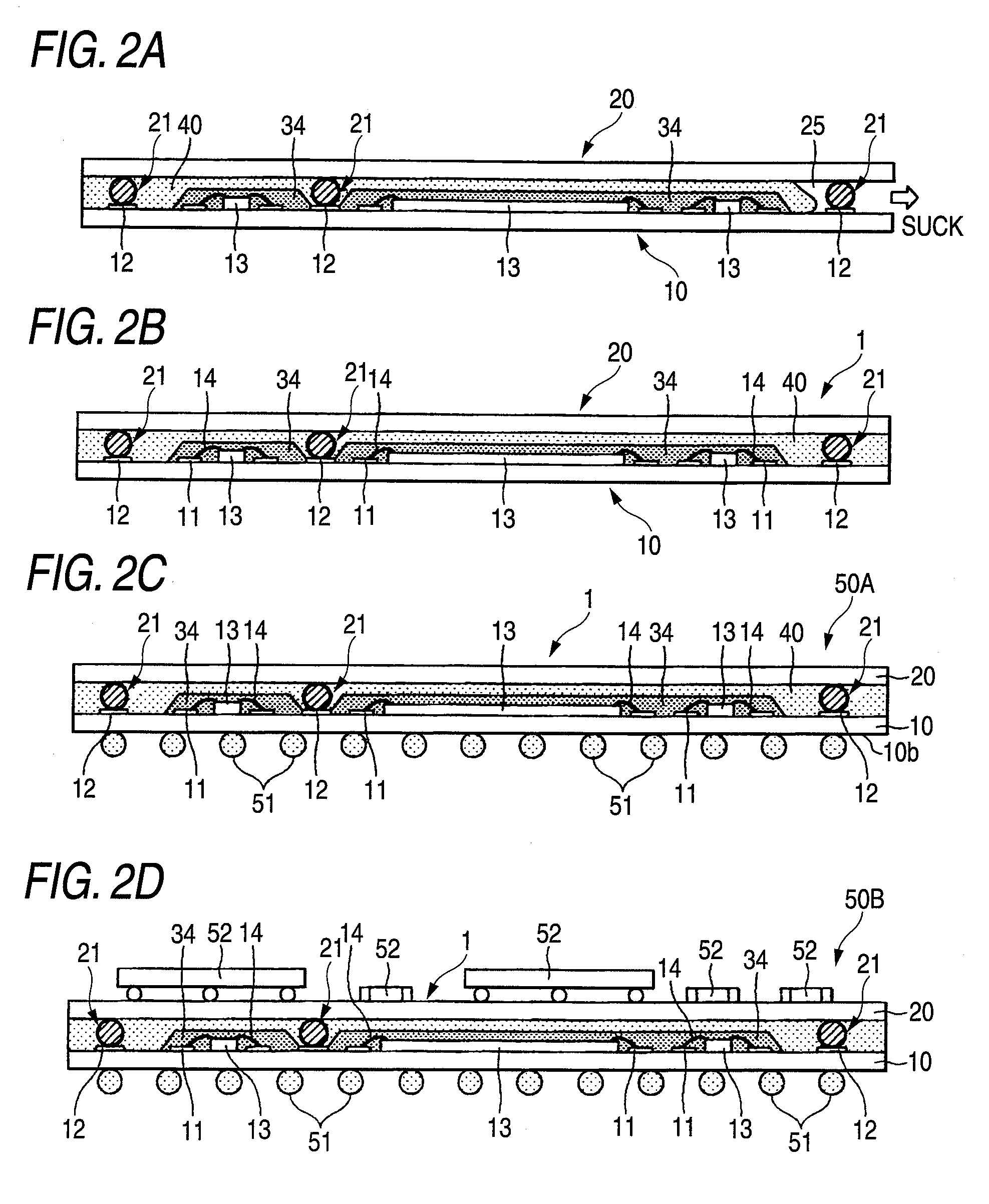
[0022]FIGS. 1 and 2 are views for explaining a method of manufacturing a chip integrated substrate according to an example of the invention in accordance with a manufacturing procedure. In particular, FIG. 2B shows a chip integrated substrate 1 which is manufactured by the manufacturing method according to the example, and a structure of the chip integrated substrate 13 will be described with reference to FIG. 2B prior to explanation of the method of manufacturing a chip integrated substrate for convenience of the description.

[0023]The chip integrated substrate 1 is roughly constituted by a first substrate 10, a second substrate 20, a chip-shaped electronic component 13 (which will be hereinafter referred to as a chip component), an electrode 21, a first sealing resin 34 and a second sealing resin 40. The first substrate 10 is a wiring board on which a wiring pattern is formed, ...


PUM


Abstract

There are provided the steps of connecting a chip component 13 to a first substrate 10 through a wire 14, providing an electrode 21 on a second substrate 20, attaching, to the first substrate 10, a molding tool 30 having a protruded portion 31 formed corresponding to an array of a bump connecting pad 12 of the first substrate 10 and a cavity 32 formed corresponding to a region in which the chip component 13 is mounted, thereby forming a first sealing resin 34 for sealing the chip component 13 and the wire 14, bonding the electrode 21 to the bump connecting pad 12 through a solder, thereby bonding the first substrate 10 to the second substrate 20, and filling a second filling resin 40 in a clearance portion between the first substrate 10 and the second substrate 20.

Description

BACKGROUND OF THE INVENTION[0001]The present invention relates to a method of manufacturing a chip integrated substrate and more particularly to a method of manufacturing a chip integrated substrate which manufactures a chip integrated substrate having a chip provided between a pair of wiring boards.[0002]At present, a performance of an electronic apparatus using a semiconductor device including a semiconductor chip has been enhanced, and it has been demanded to increase a density in the case in which a semiconductor chip is mounted on a substrate and to reduce a size and a space of the substrate mounting the semiconductor chip thereon.[0003]Therefore, there has been proposed a substrate having a semiconductor chip embedded therein, that is, a so-called chip integrated type wiring board (hereinafter referred to as a chip integrated substrate), and there have been proposed various structures for causing the semiconductor chip to include the substrate.[0004]An example of the chip inte...

Claims


Application Information

Patent Timeline
Patent Type & Authority Applications(United States)
IPC IPC(8): H01L21/00
CPCH01L21/565H01L23/3128H01L2924/19041H01L2924/3011H05K1/144H05K3/3436H05K2201/10234H05K2201/10977H05K2203/1322H01L2224/16225H01L2224/48227H01L2924/15311H01L2924/15331H01L2924/19105H01L2224/32225H01L2224/73265H01L2924/00012H01L2224/45144H01L2924/00H01L24/73
Inventor KOBAYASHI, TOSHIO
Owner SHINKO ELECTRIC IND CO LTD
Why Eureka
Try Eureka