

Lead frame and manufacturing method thereof, and semiconductor apparatus and manufacturing method thereof
- Summary
- Abstract
- Description
- Claims
- Application Information
AI Technical Summary
Benefits of technology
Problems solved by technology
Method used
Image

Examples
Embodiment Construction
[0067]Hereunder, a specific embodiment of the present invention is described with reference to the drawings.
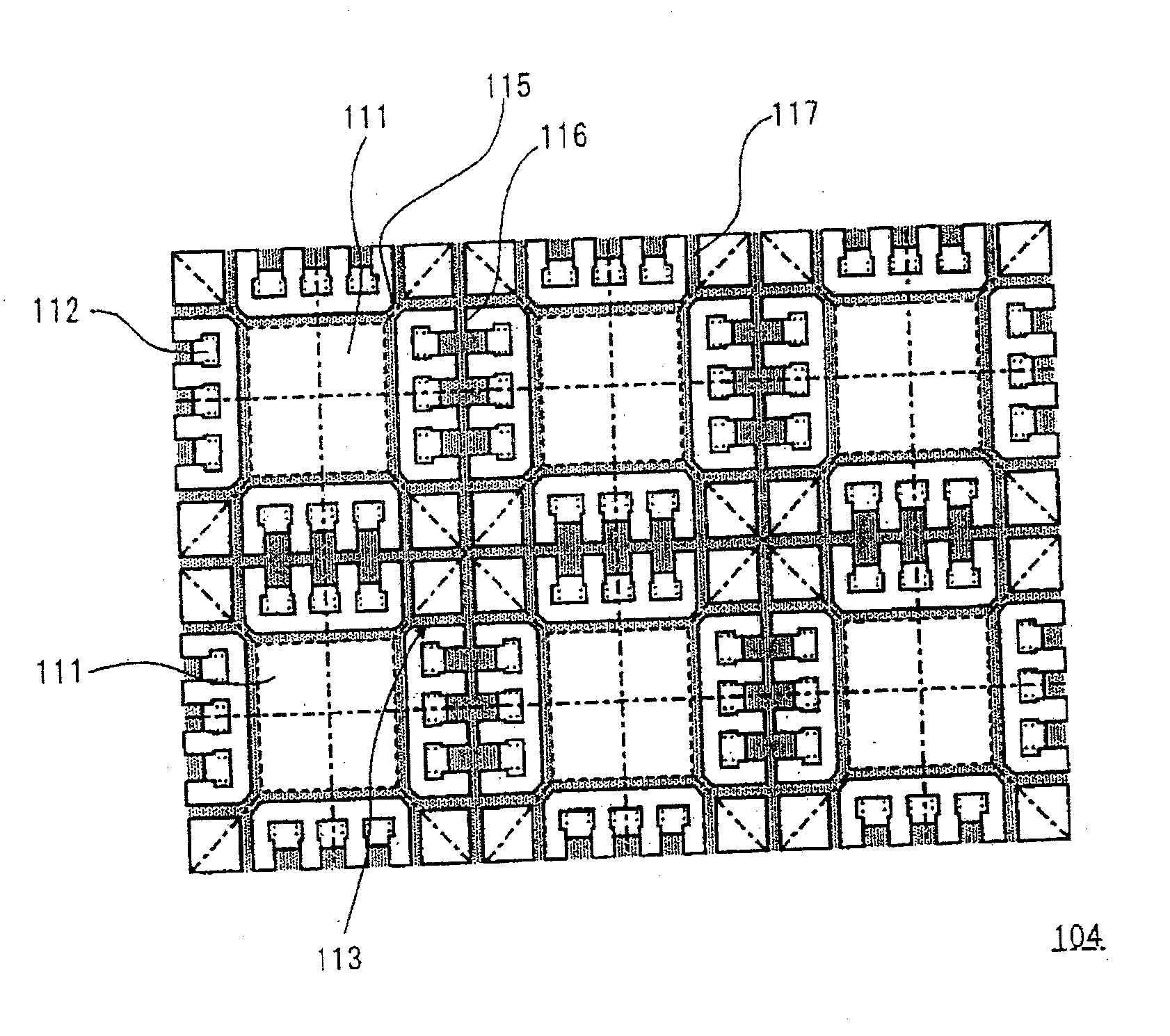
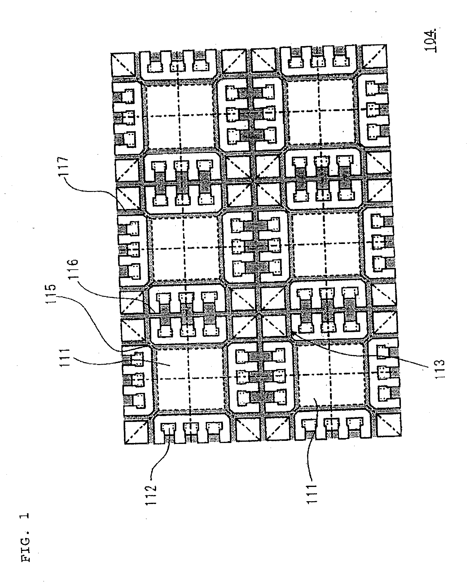
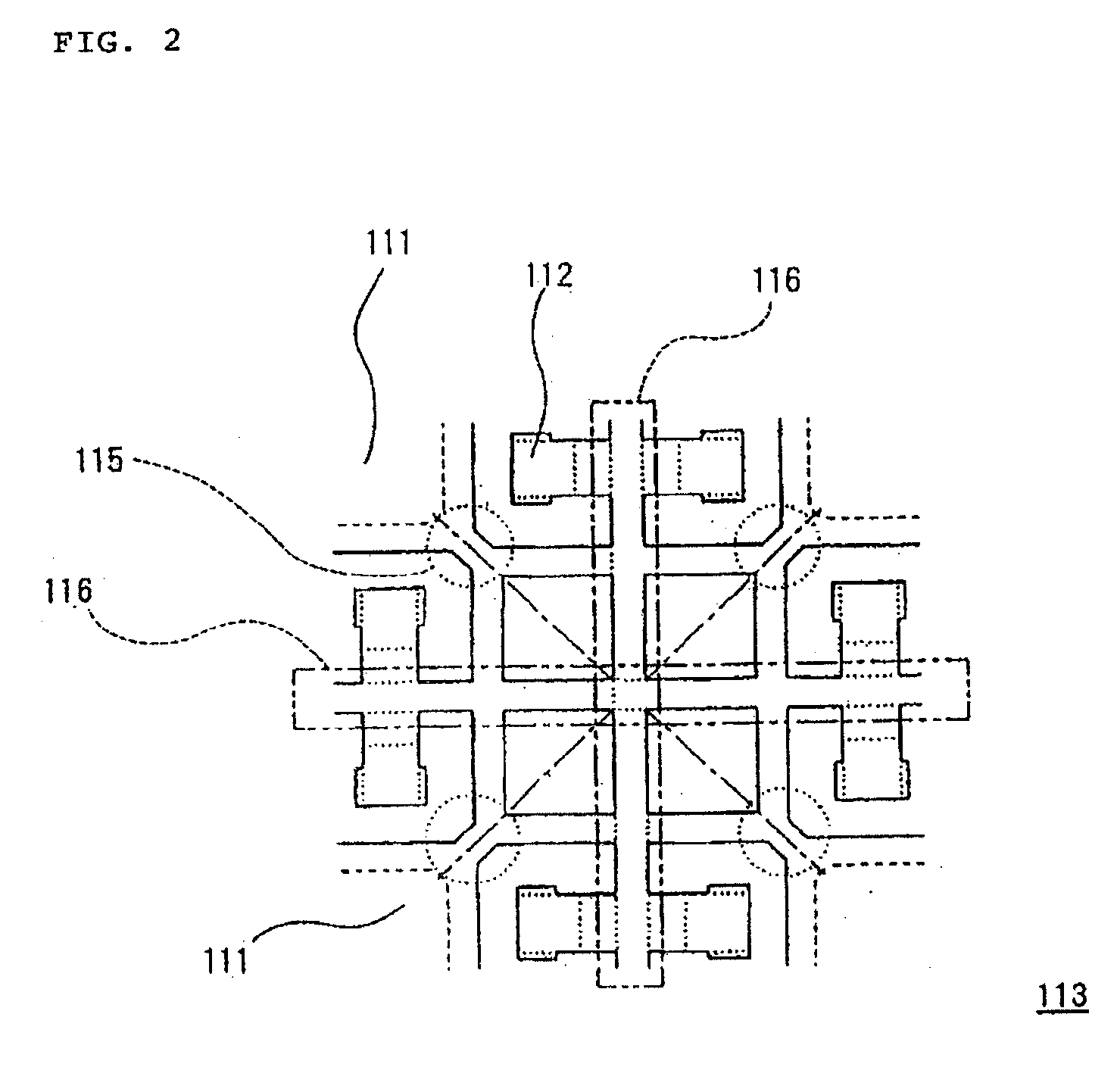
[0068]As shown in FIG. 7, lead frame 4 of the present embodiment comprises a plurality of mounting portions 11 on which semiconductor elements 3 are mounted, a plurality of electrodes 12 to which terminals of semiconductor elements 3 that are mounted on mounting portions 11 are electrically connected, and corner portions 13 that extend outward from each mounting portion 11 to connect a plurality of mounting portions 11. Components that are equivalent to a plurality of semiconductor packages are arranged on one lead frame 4.
[0069]Lead frame 4 illustrated in FIG. 7 is a configuration example for a 12-pin semiconductor package in which a pattern that is equivalent to the amount for a single semiconductor package is formed by single mounting portion 11 and a total of 12 electrodes 12. Three electrodes 12 are provided on each side of the outer circumference of mounting portion 11. ...
PUM
| Property | Measurement | Unit |
|---|---|---|
| Fraction | aaaaa | aaaaa |
| Fraction | aaaaa | aaaaa |
| Thickness | aaaaa | aaaaa |
Abstract
Description
Claims
Application Information