

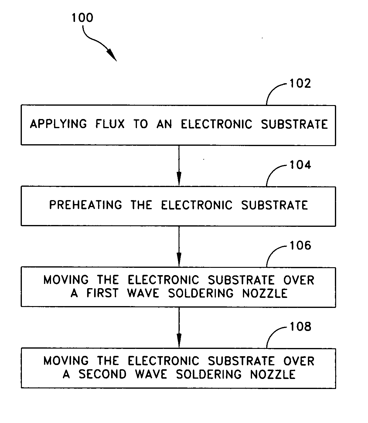
Method and apparatus for wave soldering an electronic substrate
a wave soldering and electronic substrate technology, applied in the direction of welding apparatus, welding apparatus, manufacturing tools, etc., can solve the problems of lead-free soldering, increased process costs, and reduced process yields, and the ability of currently available equipment and process techniques to accommodate lead-free solders and newer and more challenging products, regardless of the solder alloy, are limited
- Summary
- Abstract
- Description
- Claims
- Application Information
AI Technical Summary
Benefits of technology
Problems solved by technology
Method used
Image

Examples
Embodiment Construction
[0023]This invention is not limited in its application to the details of construction and the arrangement of components set forth in the following description or illustrated in the drawings. The invention is capable of other embodiments and of being practiced or of being carried out in various ways. Also, the phraseology and terminology used herein is for the purpose of description and should not be regarded as limiting. The use of “including,”“comprising,”“having,”“containing,”“involving,” and variations thereof herein, is meant to encompass the items listed thereafter and equivalents thereof as well as additional items.
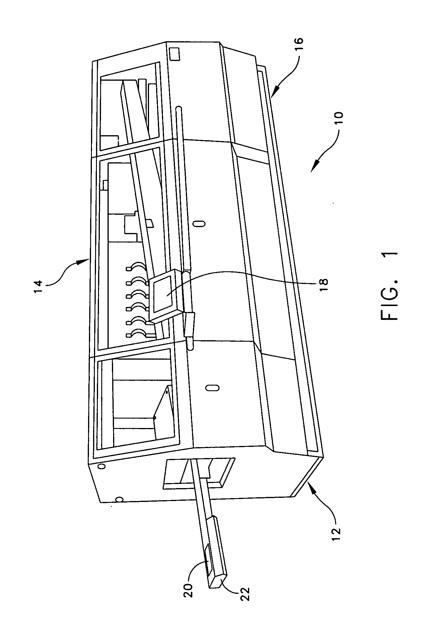
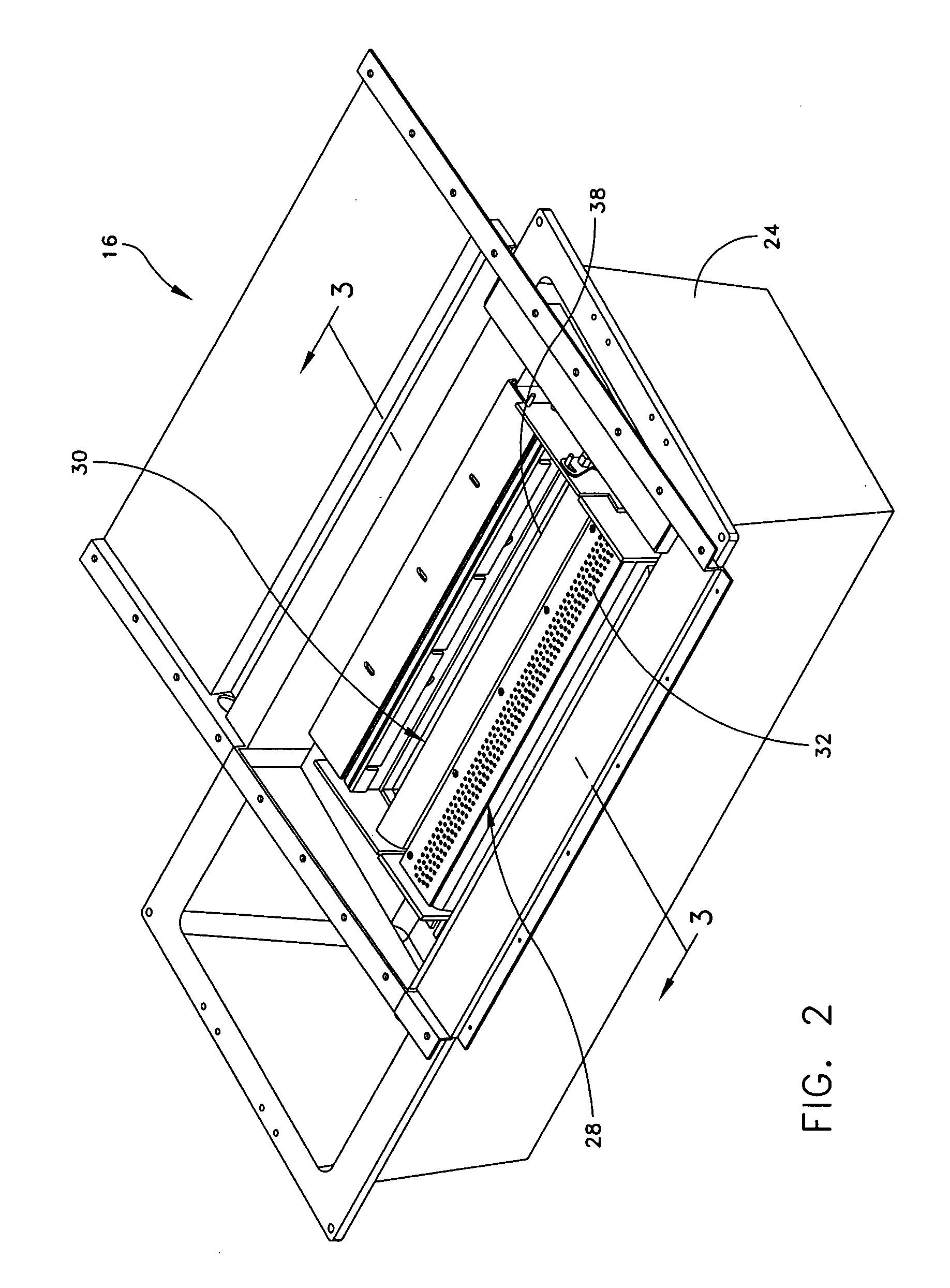
[0024]Generally speaking, wave soldering incorporates a wave soldering machine in which molten solder is pumped up to form at least one standing wave while electronic substrates are passed over the wave, thereby forming many solder joints that are uniform. Such wave soldering machines are designed to perform soldering operations at a high efficiency. The wave solder...
PUM
| Property | Measurement | Unit |
|---|---|---|
| temperature | aaaaa | aaaaa |
| widthwise dimension | aaaaa | aaaaa |
| thickness | aaaaa | aaaaa |
Abstract
Description
Claims
Application Information