Three-dimensional package structure

a package structure and three-dimensional technology, applied in the field of package structure, can solve the problems of affecting the operation of the control device, the surface occupied by the device is pretty large, etc., and achieve the effects of reducing the size of the package structure, reducing the emi, and improving the heat dissipation ability

Active Publication Date: 2008-12-11
CYNTEC
View PDF12 Cites 56 Cited by
  • Summary
  • Abstract
  • Description
  • Claims
  • Application Information

AI Technical Summary

Benefits of technology

[0009]Another object of the present invention is to provide a three-dimensional package structure having a shielding layer to inhibit or reduce EMI.
[0010]Further another object of the present invention is to provide a three-dimensional package structure in which an energy storage element is stacked on a semiconductor package body to reduce the size of the package structure.
[0011]Further another object of the present invention is to provide a three-dimensional package structure to improve the heat-dissipating ability.
[0012]Further another object of the present invention is to provide a three-dimensional package structure applicable to a POL converter in which devices except a choke coil are packaged inside a semiconductor package body and the choke coil is disposed on the semiconductor package body to be a three-dimensional package structure to reduce the size of the package structure.

Problems solved by technology

Therefore, the surface occupied by the devices is pretty large.
Furthermore, during the operation of the choke coil 15, electric and magnetic are generated which can interfere with the operation of the control device 11.

Method used


Image

  • Three-dimensional package structure
  • Three-dimensional package structure
  • Three-dimensional package structure

Examples


Embodiment Construction

[0022]Some embodiments of the invention will now be described in greater detail. Nevertheless, it should be noted that the present invention can be practiced in a wide range of other embodiments besides those explicitly described, and the scope of the present invention is expressly not limited except as specified in the accompanying claims.

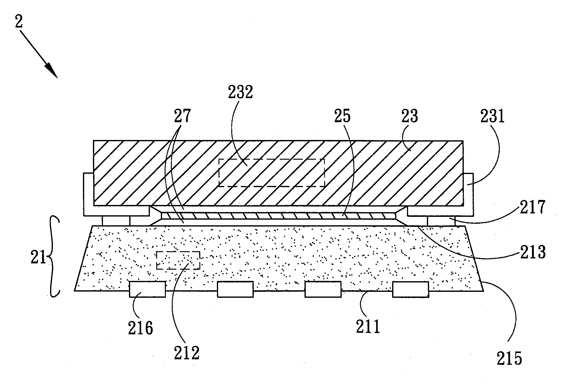
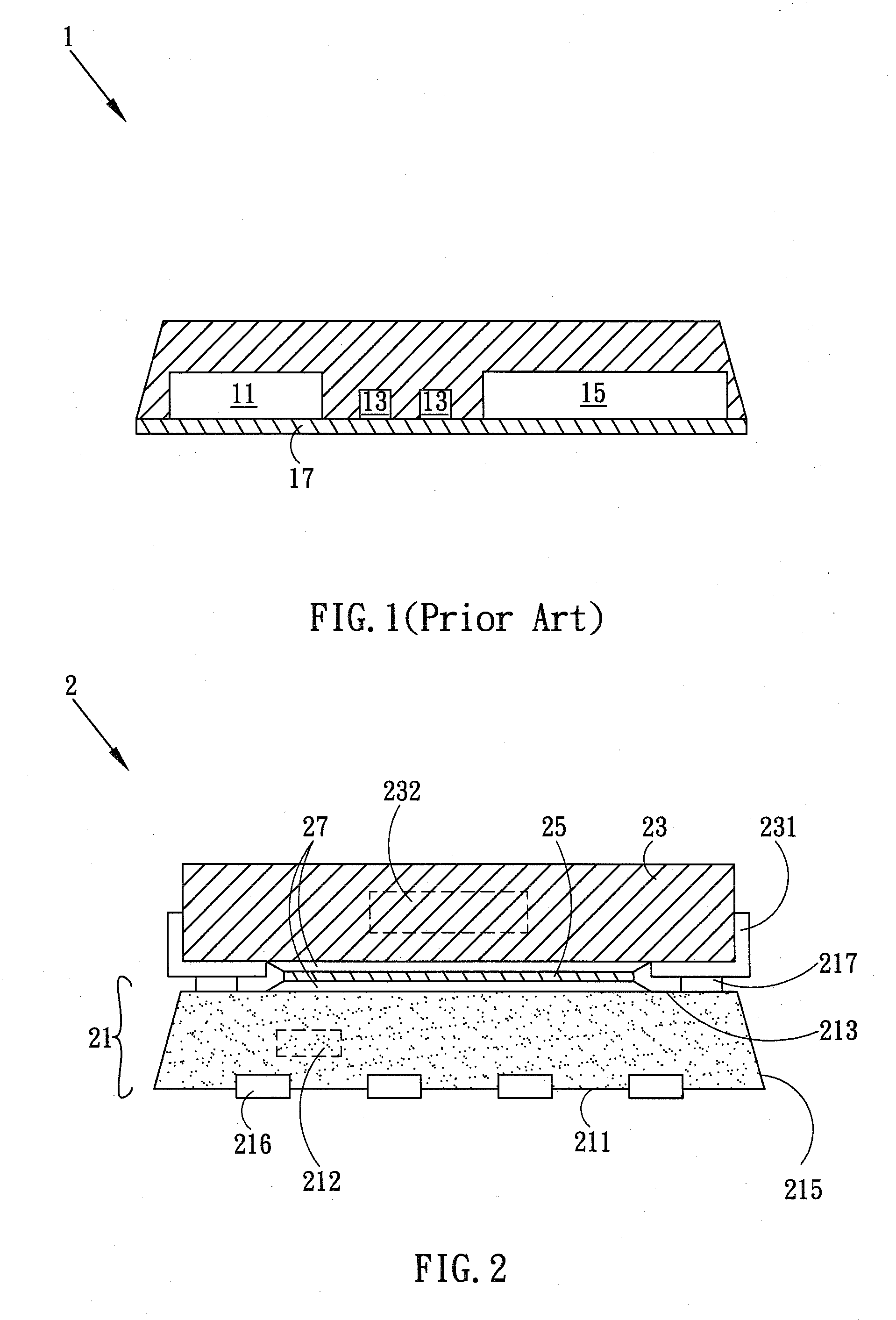
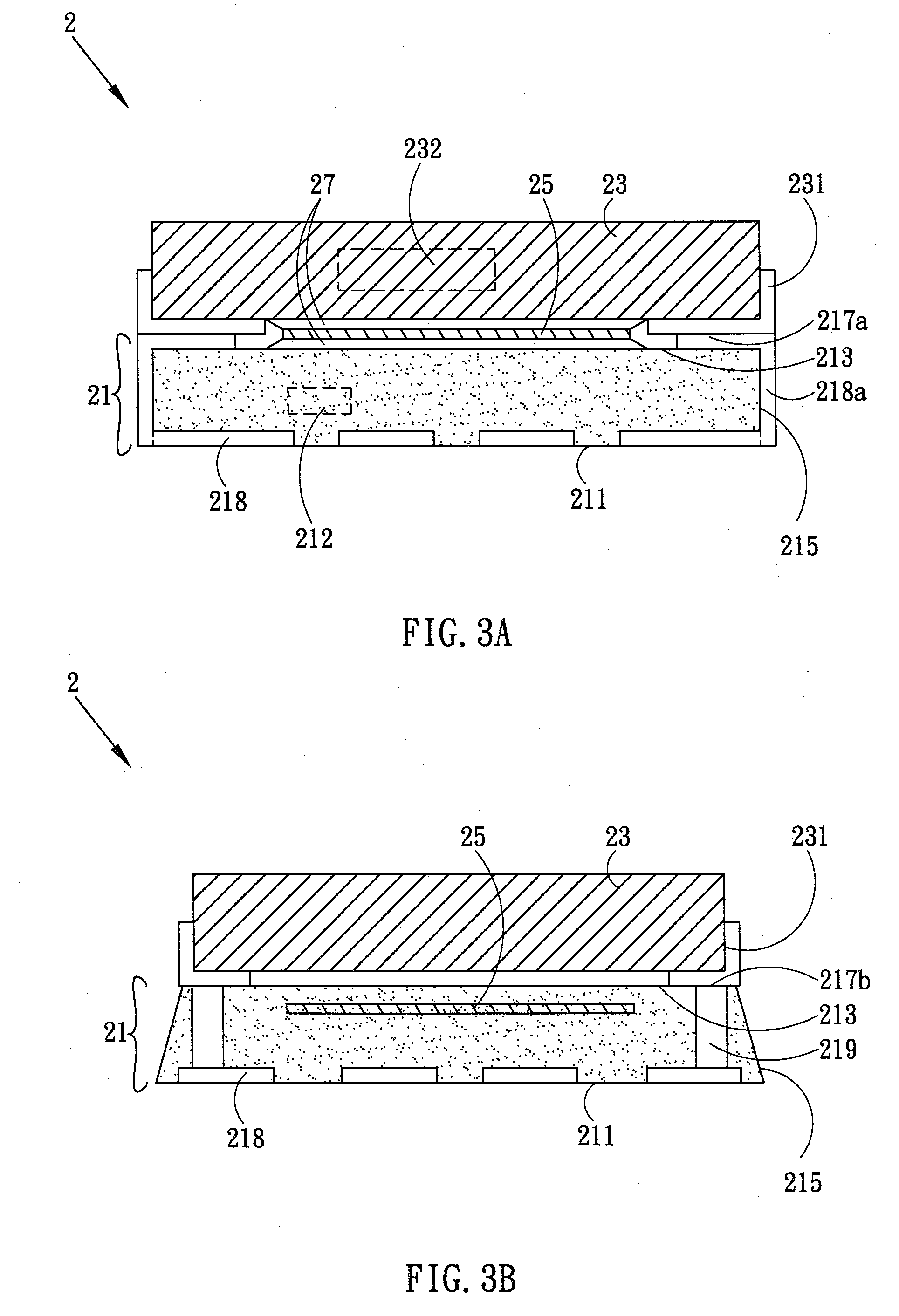
[0023]As shown in FIG. 2, according to an embodiment of the present invention, a three-dimensional package structure 2 includes a semiconductor package body 21, an energy storage element 23 and a shielding layer 25. The semiconductor package body 21 has a first surface 213, a second surface 211 opposite the first surface 213, and a sidewall 215 interconnecting the first surface 213 and the second surface 211. The semiconductor package body 21 has a plurality of first conductive elements 216 on the second surface 211 or the sidewall 215 to be electrically connected to an outside device (not shown), such as a mother board. The first conductive eleme...


PUM


Abstract

A three-dimensional package structure includes an energy storage element, a semiconductor package body and a shielding layer. The semiconductor package body has a plurality of second conductive elements and at least one control device inside. The energy storage element is disposed on the semiconductor package body. The energy storage element including a magnetic body is electrically connected to the second conductive elements. The semiconductor package body or the energy storage element has a plurality of first conductive elements to be electrically connected to an outside device. The shielding layer is disposed between the control component and at least part of the magnetic body to inhibit or reduce EMI (Electro-Magnetic Interference) from the energy storage element and to get a tiny package structure. The three-dimensional package structure is applicable to a POL (Point of Load) converter.

Description

BACKGROUND OF THE INVENTION[0001]1. Field of the Invention[0002]The present invention generally relates to a package structure, and more particularly to a three-dimensional package structure.[0003]2. Description of the Prior Art[0004]Increasing device complexity but shrinking size is common trend of electrical products. How to put more electrical elements or circuits into a limited space is important for electrical products' designers. Therefore, a three-dimensional package structure is a method to increase the density of the electrical products.[0005]Point-of-Load (POL) converter also can be called as DC / DC converter. A conventional POL converter is packaged by BGA (Ball Grid Array) package or LGA (Land Grid Array) package.[0006]As shown in FIG. 1, a conventional POL converter 1 includes at least one control device 11, at least one MOSFET 13 and a choke coil 15. Take BGA package for example. The control device 11 and the MOSFET 13 and the choke coil 15 are electrically connected to...

Claims


Application Information

Patent Timeline
Patent Type & Authority Applications(United States)
IPC IPC(8): H01L23/495
CPCH01L23/495H01L23/49555H01L23/49575H01L23/552H01L2224/48091H01L2924/19041H01L2924/19105H01L2924/3025H01L2924/00014H01L24/48H01L2924/13091H01L2924/181H01L2924/00012H01L2224/45099H01L2224/45015H01L2924/207
Inventor CHEN, DA-JUNGLIU, CHUN-TIAOWEN, CHAU-CHUN
Owner CYNTEC
Why Eureka
Try Eureka