Liquid crystal display device and method for driving the same
a liquid crystal display and display device technology, applied in the field of display devices, can solve the problems of inability to overcome the distortion the difference in distortion voltage may be great between the center and the periphery, and the inability to compensate the deviation of the common voltage vcom. to achieve the effect of reducing the compensating deviation of the common voltag
- Summary
- Abstract
- Description
- Claims
- Application Information
AI Technical Summary
Benefits of technology
Problems solved by technology
Method used
Image
Examples
first embodiment
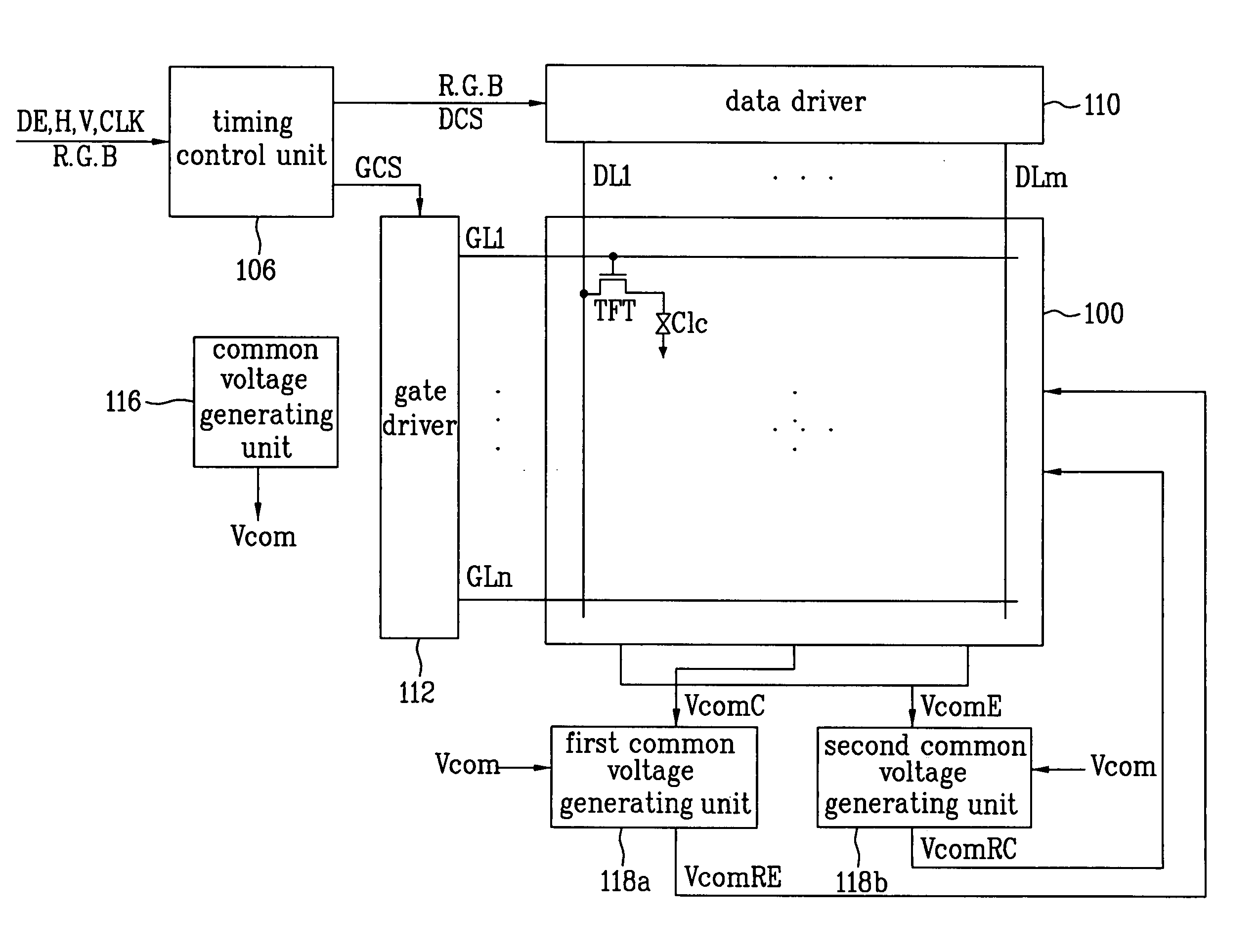
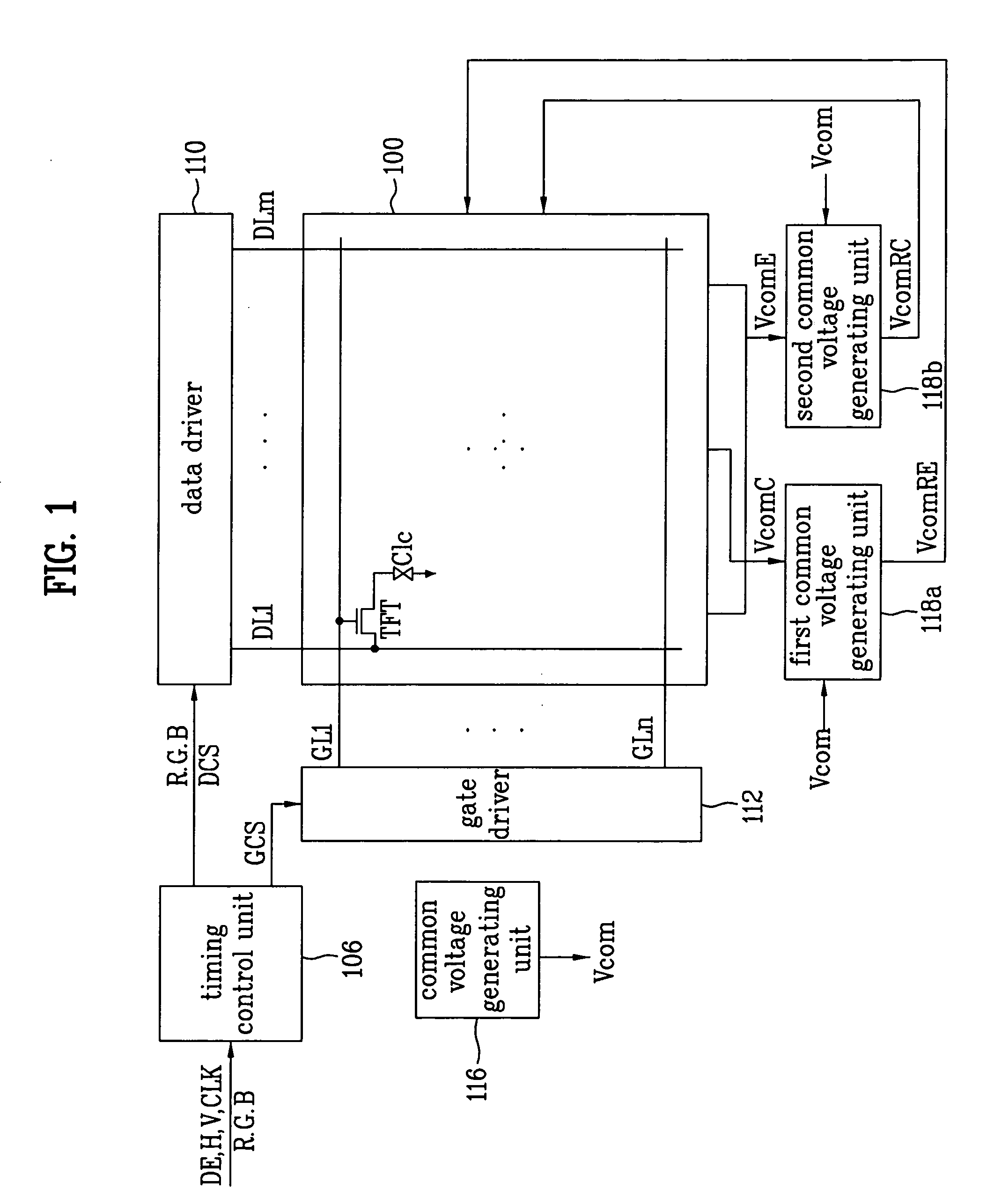
[0025]FIG. 1 is a block diagram of a liquid crystal display device in accordance with the present invention.
[0026]Referring toFIG. 1, the liquid crystal display device includes a liquid crystal display panel 100, a data driver 110 for supplying a data voltage to data lines DL1 to DLm of the liquid crystal display panel 100, a gate driver 112 for driving gate lines GL1 to GLn of the liquid crystal display panel 100 in succession, a timing control unit 106 for controlling the data driver 110 and the gate driver 112, a common voltage generating unit 116 for generating a common voltage for driving the liquid crystal display panel 100, and first and second common voltage compensating units 118a and 118b for compensating for distortion of the common voltage Vcom.
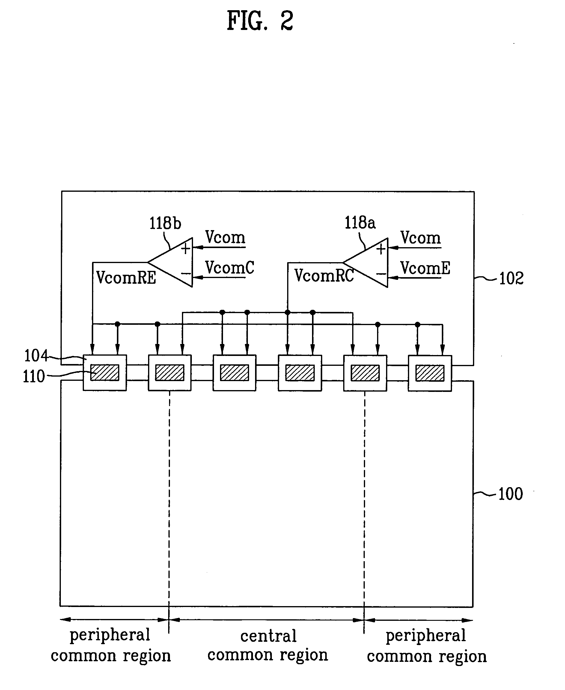
[0027]Referring to FIG. 3, the liquid crystal display panel 100 includes a thin film transistor TFT substrate 101 having a plurality of gate lines GL1 to GLn that cross data lines DL1 to DLm, a color filter substrate 103 having th...
second embodiment
[0040]A liquid crystal display device in accordance with the present invention is identical to the embodiment illustrated in FIG. 2, except that the common electrode is divided. Therefore, the same reference numerals will be used for those components which are identical to those of FIG. 2, and a detailed description of components identical to those shown in FIG. 2 will be omitted.
[0041]FIG. 3 is a schematic diagram of a liquid crystal display device including a common voltage compensating unit in accordance with a second embodiment of the present invention.
[0042]Referring to FIG. 3, in the liquid crystal display device in accordance with a second embodiment of the present invention, the thin film transistor substrate 101 of the liquid crystal display panel 100 is identical to the foregoing embodiment, while the common electrode of the color filter substrate 103 includes a peripheral common region having a left portion 119a and a right portion 119c, and a central common region 119b. ...
PUM
 Abstract
Description
Claims
Application Information


