Power semiconductor packaging method and structure

a technology of power semiconductor and packaging structure, applied in semiconductor devices, semiconductor/solid-state device details, electrical devices, etc., can solve the problems of affecting the reliability of packaging structures, and unable to meet the requirements of continuous exposure to relatively high temperatures without facing degradation and reliability, etc., to achieve the effect of reducing parasitic capacitance and low thermal resistan

Active Publication Date: 2008-12-11
GENERAL ELECTRIC CO
View PDF21 Cites 43 Cited by
  • Summary
  • Abstract
  • Description
  • Claims
  • Application Information

AI Technical Summary

Benefits of technology

[0009]The present application is directed to various power semiconductor packaging structures and methods of making the packaging structures. The various disclosed embodiments may have one or more of the following benefits: removal of organic adhesive material and/or other organic materials that may limit device operation or cause undesirable stresses at certain elevated temperatures, during applications involving wide thermal cycles or in high moisture environments; empl...

Problems solved by technology

However, operating wide band gap power devices at high temperatures puts severe limitations on the packaging, assembly, interconnection materials, processes and structures.
Packaging structures incorporating these technologies generally cannot be subjected to continuous exposure of relatively high temperatures without facing issues of degradation and reliability.
For applications involving very cold temperatures or wide thermal cycles, the use of these organic adhesion layers may cause undesirable levels of thermal stress on packaging structures.
Using polymers in packaging structures which are not hermetically sealed may also cause problems in high moisture environments, since polymers tend to absorb moisture.
Absorption of moisture can have undesirable effects, including raising the dielectric constants of the polymers and increasing parasitic capacitances.
Packaging approaches that do not contain organic polymer materials are generally complex, costly and have poor electrical performance.
However, incorporating interconnect structures on ce...

Method used


Image

  • Power semiconductor packaging method and structure
  • Power semiconductor packaging method and structure
  • Power semiconductor packaging method and structure

Examples


Embodiment Construction

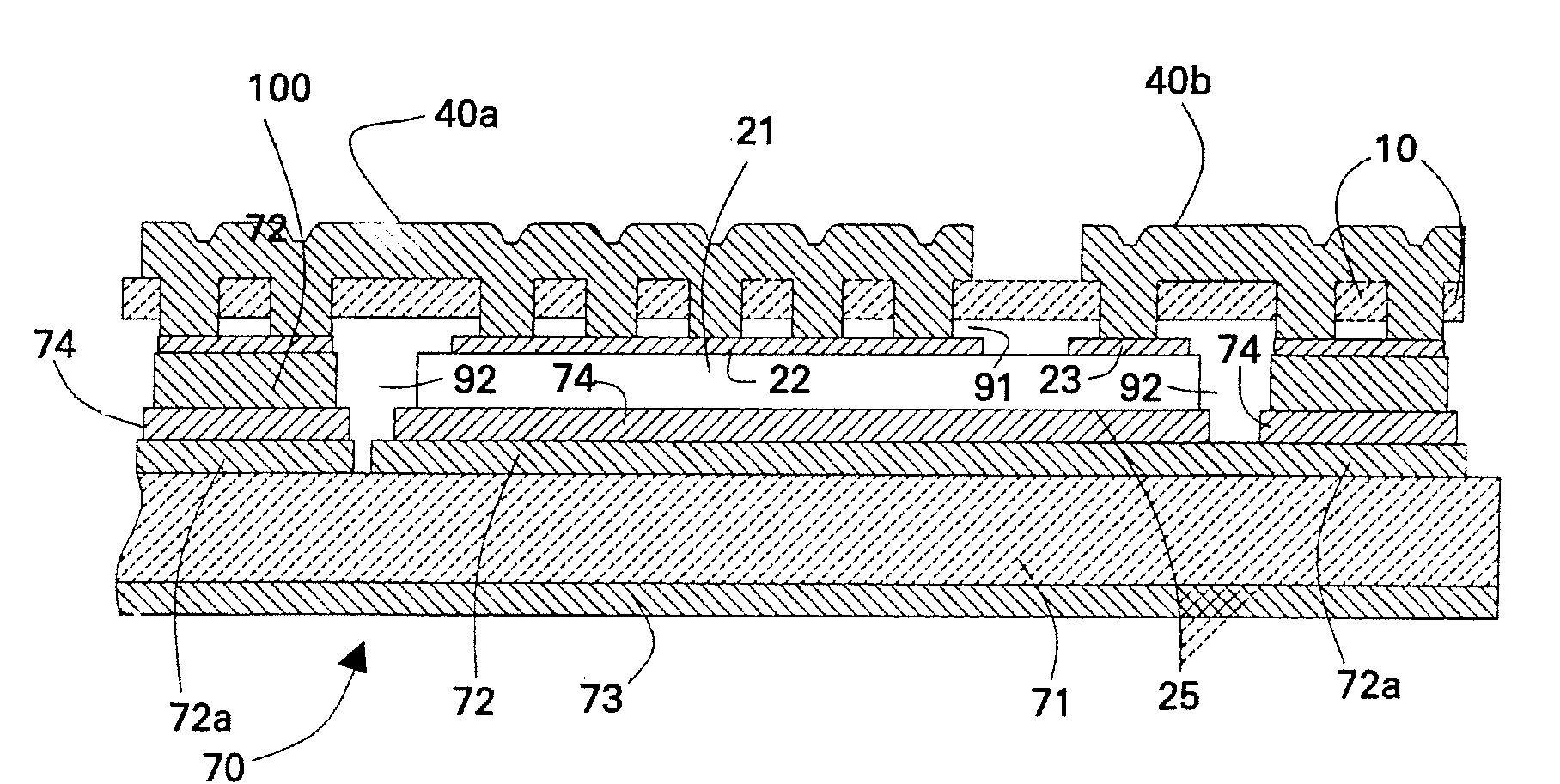
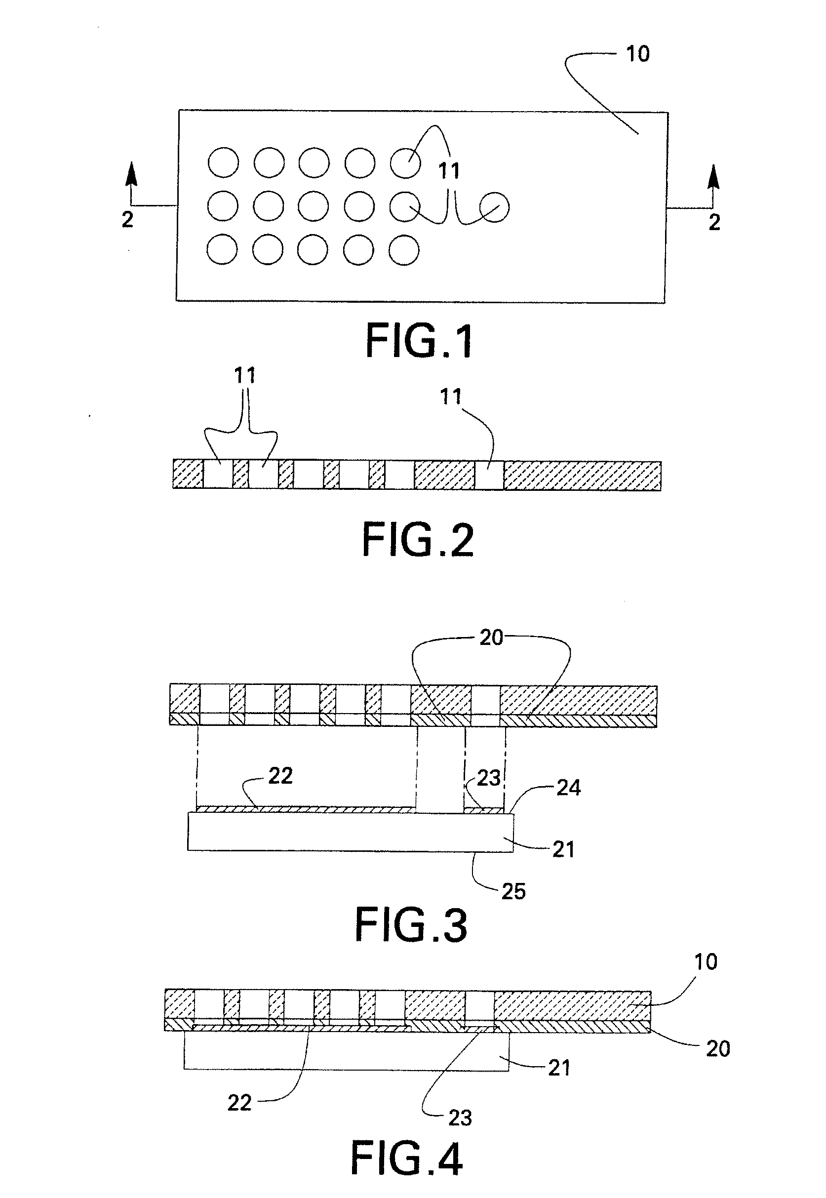
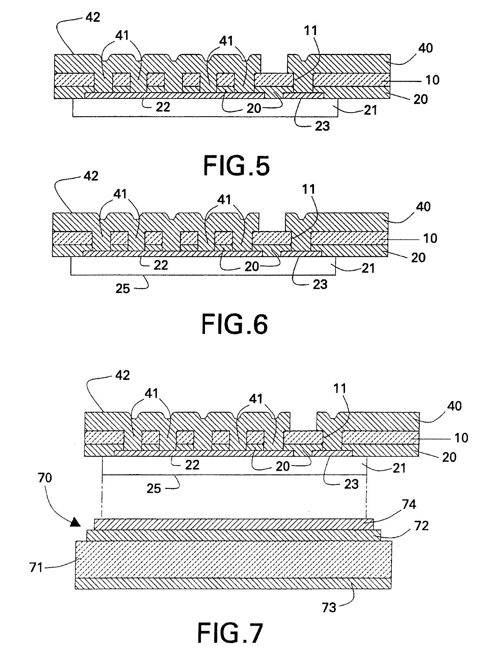
[0032]In the following description, reference is made to the accompanying drawings, which show by way of illustration specific exemplary embodiments in which the systems and techniques described may be practiced. The following description is, therefore, not to be taken in a limited sense. Wherever possible, the same reference numbers are used throughout the drawings to refer to the same or like parts.

[0033]Approximating language, as used herein throughout the specification and claims, may be applied to modify any quantitative representation that could permissibly vary without resulting in a change in the basic function to which it is related. Accordingly, a value modified by a term or terms, such as “about”, may not to be limited to the precise value specified. In at least some instances, the approximating language may correspond to the precision of an instrument for measuring the value.

[0034]The temperature at which any given semiconductor packaging structure may continuously be us...


PUM


Abstract

A semiconductor chip packaging structure is fabricated by using a dielectric film with two surfaces, and a power semiconductor chip with an active surface having contact pads. An adhesive layer is used to connect the first surface of the dielectric film and the active surface of the power semiconductor chip. A patterned electrically conductive layer is formed adjacent to the second surface of the film, extending through holes in the film to the contact pads.

Description

[0001]The present patent application is a continuation-in-part application of U.S. patent application Ser. No. 11 / 205,903 filed 17 Aug. 2005, the disclosure of which is hereby incorporated by reference in its entirety and to which the current application claims priority under 35 U.S.C. §120.BACKGROUND OF THE INVENTION[0002]The present application relates generally to structures and methods for packaging power semiconductor devices.[0003]Wide band gap semiconductor devices, such as SiC devices, have the ability to operate at highly elevated temperatures for some power electronics applications, without degrading device performance or developing failure mechanisms that would limit operating life. This attribute has the potential benefit of permitting high power operation in high temperature environments without expensive cooling structures and materials that would be required if lower operating temperatures had to be maintained. However, operating wide band gap power devices at high te...

Claims


Application Information

Patent Timeline
IPC IPC(8): H01L21/50
CPCH01L23/4821H01L23/4822H01L2924/1305H01L2224/73267H01L2224/92144H01L2924/014H01L2924/01047H01L23/5385H01L23/5389H01L24/24H01L24/82H01L24/83H01L25/072H01L2224/2402H01L2224/24226H01L2224/2518H01L2224/82039H01L2224/82047H01L2224/83801H01L2924/01004H01L2924/01013H01L2924/01027H01L2924/01029H01L2924/01032H01L2924/01042H01L2924/01046H01L2924/01049H01L2924/01061H01L2924/01074H01L2924/01078H01L2924/01079H01L2924/01082H01L2924/09701H01L2924/10329H01L2924/13055H01L2924/13091H01L2924/15787H01L2924/30105H01L2924/30107H01L2224/32225H01L2924/01006H01L2924/01019H01L2924/01023H01L2924/01033H01L2924/00H01L2924/351H01L2224/72H01L2224/06181H01L2224/0603
Inventor FILLION, RAYMOND ALBERTBEAUPRE, RICHARD ALFREDELASSER, AHMEDWOJNAROWSKI, ROBERT JOHNKORMAN, CHARLES STEVEN
Owner GENERAL ELECTRIC CO
Why Eureka
Try Eureka